← AiTimeline Home

Technology · Semiconductor Infrastructure

ASML Timeline 1984–2026: How One Dutch Company Became Essential to AI Chips

📅 Updated 8 September 2026Reuters, ASML, TSMC, Samsung NewsroomTechnology & geopolitics explainer
Advertisement

View as Web Story

In short

Explore ASML's 1984-2026 timeline: EUV lithography, High-NA EUV, AI chips, TSMC, Samsung, Intel and the semiconductor race behind every AI chip made today.

Latest Story

Every AI chatbot, data center and graphics processor depends on layers of invisible infrastructure. Nvidia may design the GPU. TSMC may manufacture it. But the microscopic circuit patterns inside the world’s most advanced chips rely on lithography systems so complex that only one company has mastered the most advanced version at scale: ASML. The strange part is that ASML does not make the chips. It makes the machines that help make the chips. This ASML timeline traces that story from a struggling 1984 startup to the single company the entire AI industry now quietly depends on.

What If ASML Stopped Making Chip Machines?

🧠 Quick Answer

ASML is a Dutch company that makes lithography systems used by semiconductor manufacturers to print microscopic circuit patterns on silicon wafers. It is the only company that makes EUV lithography machines used for leading-edge chip production. ASML does not manufacture chips itself, but its machines are essential to fabs run by companies such as TSMC, Samsung and Intel.

⚡ ASML Quick Facts
Founded1984, a Philips & ASM International joint venture
HeadquartersVeldhoven, Netherlands
EUV lithographyASML is the only company in the world that makes it
2026 revenue forecast€36–40 billion (raised April 2026, ASML)
Workforce44,500+ employees worldwide (ASML)
Biggest EUV customerTSMC — roughly 40% of EUV system deliveries
⚡ Quick Answers — AI Overview Ready

ASML: Key Questions

Does ASML manufacture computer chips?
No. ASML manufactures lithography systems used by semiconductor manufacturers. Its machines help print microscopic chip patterns, but companies such as TSMC, Samsung and Intel run the fabs that manufacture chips.
What does ASML actually do?
ASML designs and builds lithography systems — machines that project microscopic circuit patterns onto silicon wafers using light. Chipmakers buy these systems and run them inside their own fabs to manufacture semiconductors.
Why is ASML important for AI chips?
Advanced AI accelerators need extremely dense, precise circuit patterns to pack in more transistors. ASML’s EUV lithography systems are the only tools in the world capable of printing many of those patterns at the required scale.
What is EUV lithography?
Extreme ultraviolet lithography uses much shorter-wavelength light than earlier methods to print extremely small circuit features more efficiently, letting chipmakers pack far more transistors onto the same piece of silicon.
📚 Key Takeaways

What this ASML timeline really shows

  • ASML does not make chips; it makes the lithography machines used to make advanced chips. That distinction is the single most misunderstood fact about the company.
  • ASML is the only maker of EUV lithography systems used for leading-edge semiconductor production — a position built over four decades, not overnight.
  • EUV became essential because chipmakers needed to print extremely small circuit patterns to keep shrinking transistors after older lithography methods ran out of room.
  • AI-chip demand has made ASML even more strategically important, pulling the company into a capacity-expansion race it did not choose alone.
  • High-NA EUV is the next big lithography transition, but cost, mask size and integration into real fabs remain unresolved challenges, not finished work.
  • The semiconductor supply chain is an ecosystem, not a single-company story — ASML is essential, but Nvidia, TSMC, Applied Materials, Zeiss and dozens of others all matter too.
  • ASML broke ground on a major new Dutch campus, BIC North, on 8 September 2026, to expand capacity for AI-driven demand it says will keep growing.
  • Advanced lithography tools have become a geopolitical chokepoint in the U.S.-China technology rivalry, putting a mid-sized Dutch company at the center of great-power tech policy.
1. Silicon wafer — a thin, ultra-pure disc of silicon, the blank canvas every chip starts as
2. Light source — an extreme ultraviolet or deep ultraviolet light source generates the wavelength needed to print tiny features
3. ASML lithography system — projects a circuit-pattern mask onto the wafer’s photosensitive coating with extraordinary precision
4. Microscopic circuit patterns — the exposed pattern is developed, etched and built up, layer by layer
5. Repeated process steps in a fab — deposition, etching, cleaning and inspection repeat dozens of times per chip
6. AI processor — the finished logic die: a GPU, TPU or custom AI accelerator
7. Advanced packaging — the logic die is fused with memory and interconnects into one finished package
8. AI data center — the packaged chip goes into a server rack that trains or runs AI models
ASML supplies step 3. Every other step depends on a separate, equally specialised part of the industry.
🔍 How Small Are We Talking? — Zoom In
Tap a scale to compare it
A human hair is roughly 70–100 micrometers thick — about the widest thing on this scale, and still nowhere close to the features a modern chip needs.
⚠️ Illustrative comparisons, rounded for clarity. Exact feature sizes vary by chipmaker and are not all publicly disclosed.

🔬 DUV vs EUV vs High-NA EUV
Tap a generation
Deep ultraviolet lithography helped chipmakers shrink features for many generations, often using multiple patterning steps for advanced nodes.
⚠️ High-NA EUV is still in early deployment as of September 2026 — not yet standard across the industry.

Who Actually Makes an AI Chip?

Tap each link in the chain to see what it actually contributes — no single company does all of this
🔗 The AI Chip Supply Chain
Designs GPUs and AI accelerators, but usually does not manufacture them in its own fabs — it hands finished chip designs to foundries like TSMC.
⚠️ Simplified for clarity. Real supply chains involve many more specialised suppliers at every link.

An important distinction, stated plainly: ASML does not manufacture Nvidia’s chips, or anyone else’s. ASML manufactures the lithography systems that foundries such as TSMC, Samsung and Intel use inside their own fabs. Those foundries also depend on an enormous ecosystem of other equipment, materials, chemicals, process recipes, metrology systems and packaging capacity — ASML is one essential piece of that ecosystem, not the whole of it.

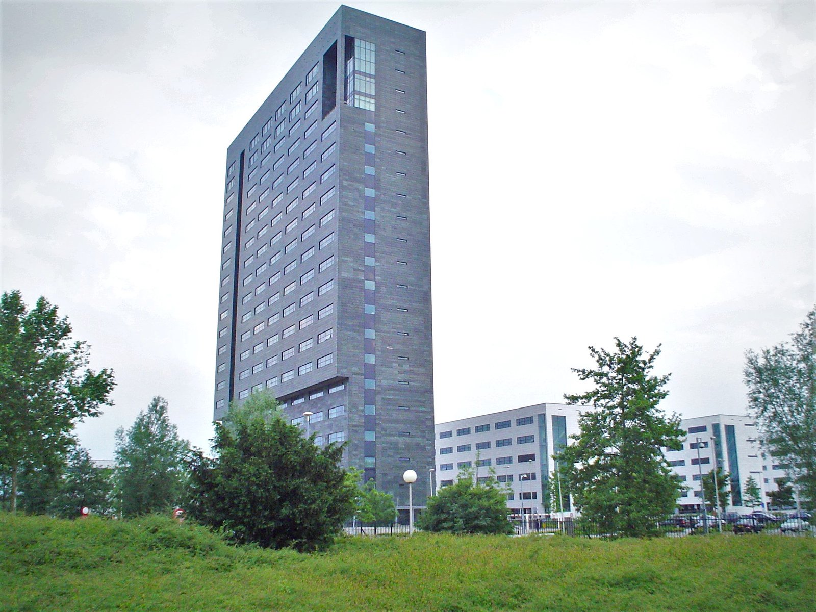
ASML corporate headquarters building in Veldhoven, Netherlands

ASML’s headquarters in Veldhoven, Netherlands — the center of a company whose machines are now essential to advanced chip production worldwide. Photo: public domain, Wikimedia Commons.

The ASML Timeline: 1984–2026

Newest first — from this week’s expansion back to a struggling 1984 startup

High-NA and future larger-mask systems — targets, not guarantees

Industry roadmapReuters reporting, September 2026

What’s targeted: Samsung and SK Hynix are targeting High-NA EUV for DRAM memory production around 2028. TSMC is looking toward advanced-node high-volume manufacturing using High-NA from around 2030. ASML aims to demonstrate larger-mask pilot capability by 2031 and broader high-volume readiness by 2033.

Why it matters: today’s EUV systems print chips up to roughly 800 square millimeters using a standard mask size; the largest AI and data-center chips are already designed right up against that limit, which is why a larger-mask generation matters.

Interesting fact: none of these dates are commitments — they are the industry’s own stated targets, and lithography roadmaps have slipped before.

ASML works on larger masks for AI data-center chips

ReutersSeptember 2026

What happened: ASML said it would partner with major chipmakers to adapt High-NA EUV systems so they can print larger chips for AI data centers — the kind of large processors Nvidia and Google design today.

The constraint: current High-NA tools use a smaller mask than standard EUV systems, which currently limits how large a chip they can print in a single exposure, even though they can resolve finer features.

Interesting fact: modern AI accelerators are already designed close to the physical reticle limit of existing EUV tools — chip size, not just feature size, has become a real engineering constraint.
8 Sep
2026

ASML breaks ground on major Dutch manufacturing expansion

ReutersBIC North, near Veldhoven/Eindhoven

What happened: ASML held a groundbreaking ceremony for a new campus at Brainport Industries Campus North, on roughly 35 hectares of undeveloped land near Eindhoven Airport, about 7km from ASML’s Veldhoven headquarters. The project will eventually span about 350,000 square meters with potential capacity for up to 20,000 workplaces.

Why now: CEO Christophe Fouquet said “the growing global demand from the semiconductor industry requires continuous investments” — AI-driven chip demand is the direct pressure behind the expansion.

~350,000 m² plannedUp to 20,000 workplaces

High-NA EUV begins the next generation

Intel, ASMLHillsboro, Oregon & global rollout

What happened: Intel installed one of the industry’s first commercial High-NA EUV systems, the ASML TWINSCAN EXE:5000, in 2024. In 2026, ASML confirmed Intel had become the first company to ship high-volume logic chips — select layers of its 18A-node Panther Lake processors — made using High-NA EUV.

Status: this is early, real deployment, not industry-wide adoption. Samsung and TSMC are still evaluating and planning their own High-NA rollouts on the later timelines described above.

Interesting fact: Intel’s early layers were “dual-qualified” — exposed on either the older 0.33 NA EUV scanner or the new 0.55 NA High-NA scanner, with interchangeable results, a deliberate hedge during the transition.
2020s

Semiconductor manufacturing becomes geopolitical

Dutch & U.S. export policyOngoing

What happened: as U.S.-China technology tensions escalated, the Dutch government — under sustained U.S. pressure — began restricting ASML’s ability to export its most advanced EUV and later some DUV systems to China. ASML had already been barred from shipping EUV machines to Chinese customers for years before these controls tightened further.

Why it matters: because ASML is the sole source for EUV lithography, its export licenses effectively function as a global chokepoint on where the most advanced chips can be made — a lever no chip designer or foundry alone controls.

Interesting fact: a single company’s export-license paperwork now shapes national semiconductor strategy in Washington, Beijing and The Hague alike.
2020s

AI accelerators increase demand for leading-edge chips

Industry-wide2022–2026

What happened: the rapid growth of large AI models and cloud AI infrastructure sharply increased demand for the most advanced GPUs and AI accelerators — and therefore for the leading-edge fabs and lithography capacity needed to build them.

The simple chain: AI models need GPUs. GPUs need advanced chips. Advanced chips need fabs. Leading-edge fabs need lithography — and for the most advanced nodes, that means ASML.

Interesting fact: ASML raised its 2026 revenue forecast to €36–40 billion in April 2026, citing AI-chip demand, and planned to ship 60 low-NA EUV tools that year — a 25% increase over 2025.

TSMC, Samsung and Intel adopt EUV

TSMC, Samsung, IntelLeading-edge nodes

What happened: TSMC and Samsung began using EUV lithography in high-volume production for their most advanced process nodes around this period, with Intel following a more delayed path into EUV adoption for its own leading-edge manufacturing.

Why it mattered: this was the moment EUV moved from a research promise to a real production tool, validating decades of ASML investment and making EUV systems the must-have equipment for any foundry chasing the leading edge.

Interesting fact: exact node-by-node adoption details vary by company and are not all fully public — foundries treat their precise EUV usage as competitively sensitive information.
2010s

EUV approaches commercial production

ASML & major foundriesR&D to early deployment

What happened: after years of research-stage development, EUV systems moved toward genuine commercial readiness during the 2010s, with major chipmakers investing directly in ASML and preparing their fabs to eventually use EUV for advanced-node manufacturing.

Why it took so long: EUV light is absorbed by almost everything, including air, which meant ASML had to develop an entirely new class of vacuum-based optics, mirrors and light sources — nothing about it could simply be adapted from earlier lithography.

Interesting fact: TSMC, Samsung and Intel all took direct equity stakes in ASML during this period specifically to help fund EUV’s development — an unusual move for competing chipmakers to make together.
2000s

The long EUV bet

ASML, Cymer, ZeissHigh-risk R&D era

What happened: ASML committed to a multi-billion-dollar, multi-decade bet on extreme ultraviolet lithography, working with partners including light-source maker Cymer (later acquired by ASML) and optics specialist Zeiss to solve problems that had never been solved commercially before.

The scale of the challenge: EUV required powerful, reliable light sources, extraordinarily precise mirror-based optics (since EUV light cannot pass through conventional lenses), and vacuum systems — coordinated across the entire semiconductor ecosystem, not just inside ASML.

Interesting fact: for much of the 2000s, EUV was widely seen inside the industry as a technology that might never become commercially viable at all.
1990s–
2000s

Deep-ultraviolet lithography advances

Industry-wideDUV & immersion lithography

What happened: deep ultraviolet lithography, and later immersion lithography — which uses a layer of water to effectively shrink the wavelength of light in use — let chipmakers keep shrinking features well beyond what many had expected DUV could achieve.

Why it matters: DUV and immersion lithography were the stepping stones that kept Moore’s Law alive while EUV was still being developed, and multi-patterning techniques stretched DUV’s usable life even further.

Interesting fact: DUV lithography, refined over decades, is still in wide use today for many chip layers — EUV replaced it only where DUV genuinely could not keep up.
1990s

Semiconductor features keep shrinking

Industry-wideMoore’s Law era

What happened: chipmakers needed to print smaller and smaller circuit patterns to fit more transistors into each chip — the pattern later popularized as Moore’s Law, describing roughly regular doublings in transistor density over time.

Why it mattered for ASML: every generation of shrinkage demanded a new generation of lithography precision, turning ASML’s core business into a permanent, compounding engineering race rather than a one-time product line.

Interesting fact: the pressure to keep shrinking features is the single force that connects ASML’s entire 40-year history — from its earliest machines to High-NA EUV today.
Late 1980s–
1990s

ASML competes with Japanese lithography leaders

Nikon, CanonMarket entry era

What happened: Nikon and Canon were the dominant, well-established lithography equipment makers when ASML entered the market. ASML had to earn trust from chipmakers through engineering reliability and close customer partnerships rather than incumbency.

Why it mattered: this early period of hard competition against better-resourced Japanese rivals shaped ASML’s later willingness to make an outsized, high-risk bet on EUV when the opportunity came — a smaller challenger had more reason to gamble on a technology leap.

Interesting fact: for years, few in the industry expected the smaller Dutch entrant to eventually out-compete both established Japanese lithography leaders.

ASML is founded

Philips & ASM InternationalVeldhoven, Netherlands

What happened: ASML began as a joint venture between electronics giant Philips and semiconductor-equipment company ASM International, entering a lithography-equipment market that was already difficult and dominated by larger, established players.

Why it matters: nothing about ASML’s origin predicted its later monopoly on EUV. It started small, under-resourced relative to its Japanese rivals, inside a struggling Dutch electronics conglomerate’s spin-off.

Interesting fact: ASML’s earliest years were genuinely uncertain — this was not an inevitable success story from day one.

ASML, TSMC, Samsung, Intel and Nvidia — Who Does What

The company profiles behind this chain, and why none of them can replace another

Equipment maker

ASML

The Dutch company that makes the lithography systems chipmakers use to print circuit patterns — the only maker of EUV lithography machines in the world. It does not design or manufacture chips.

Chip designer

Nvidia

Designs GPUs and AI accelerators used across the AI industry, but does not manufacture them in its own fabs — it relies on foundries like TSMC to turn its designs into physical chips.

Foundry

TSMC

The Taiwanese contract manufacturer that fabricates chips for customers including Nvidia and Apple, using advanced process nodes — and ASML’s biggest single EUV customer, accounting for roughly 40% of EUV deliveries.

Integrated device maker

Samsung

Runs its own foundry and memory business, using EUV for both logic chips and, increasingly, memory production — and is among the first customers targeting High-NA EUV for DRAM by 2028.

Integrated device maker

Intel

Both designs and manufactures its own chips through Intel Foundry, and became the first company to ship high-volume logic chips made using ASML’s High-NA EUV technology, on its 18A node.

Equipment ecosystem

Applied Materials, Lam Research, Tokyo Electron

Supply the deposition, etching, cleaning and other fabrication tools that surround lithography inside a fab — a reminder that ASML is one essential vendor among many, not the whole toolchain.

Lithography Generations, Side by Side

DUV, EUV and High-NA EUV compared

GenerationWhat changedStatus as of Sept 2026
DUVDeep ultraviolet light, later combined with immersion and multi-patterning techniques to print smaller features across many process generationsMature, still widely used for most chip layers
EUVExtreme ultraviolet light at a much shorter wavelength, printing the smallest leading-edge features in a single exposureMature and in high-volume production at TSMC, Samsung and Intel
High-NA EUVHigher numerical-aperture optics for finer resolution than standard EUV, currently limited by a smaller mask sizeEarly deployment — live at Intel; Samsung, SK Hynix and TSMC still on adoption roadmaps

High-NA EUV: Who’s Adopting It, and When

Company-stated targets, per Reuters reporting — plans, not guarantees

CompanyTargetUse case
IntelAlready shipping (2026)High-volume logic chips, select 18A-node Panther Lake layers
SamsungBy 2028High-volume DRAM memory production
SK HynixTargeting 2028Commercial DRAM output; also evaluating a 12-inch mask consortium
TSMCFrom around 2030Advanced-node, high-volume manufacturing
ASML (larger-mask systems)Pilot by 2031, high-volume by 2033Larger-chip printing for AI/data-center-scale processors

Beyond ASML: The Rest of the Equipment Ecosystem

A fab is not one machine — it’s dozens of specialised toolmakers working together

CategoryExample companiesRole
LithographyASMLPrints circuit patterns onto the wafer
DepositionApplied Materials, Tokyo ElectronBuilds up thin material layers on the wafer
EtchingLam Research, Tokyo ElectronRemoves material precisely to shape circuit structures
Inspection & metrologyKLADetects defects and measures pattern accuracy
Optics & light sourceZeiss, Cymer (an ASML subsidiary)Supplies the mirrors and light sources ASML’s systems depend on

💡 Worth Knowing

  • EUV light is absorbed by almost everything, including ordinary air — ASML’s EUV systems operate in a near-vacuum, using mirrors instead of the glass lenses older lithography relies on.
  • TSMC, Samsung and Intel all took direct equity stakes in ASML during EUV’s development era specifically to help fund a technology none of them could build alone.
  • ASML’s EUV systems are reportedly among the most complex machines ever built for volume manufacturing, involving hundreds of thousands of individual parts.
  • The Netherlands restricting ASML’s exports to China, under sustained U.S. pressure, shows how a single mid-sized company’s shipping decisions can shape great-power technology policy.
  • ASML is not a chip designer, a foundry, or a memory maker — it is best understood as the one company every leading-edge chipmaker on Earth currently has to buy from.

Explore More Timelines

People Also Ask

Why does Nvidia depend on ASML machines?
Nvidia designs its GPUs but does not manufacture them. Its chips are fabricated by foundries such as TSMC, which use ASML’s EUV lithography systems to print the extremely dense circuit patterns Nvidia’s designs require. Without EUV-capable fabs, Nvidia’s most advanced designs could not be physically manufactured at the density it needs.
How does TSMC use ASML machines?
TSMC installs ASML’s EUV and High-NA EUV lithography systems inside its own fabs and operates them as part of a much longer manufacturing process that also includes deposition, etching, cleaning and inspection steps from other equipment makers.
Why can’t other companies easily copy ASML?
EUV lithography required decades of compounding engineering knowledge across light sources, vacuum-based optics, mirrors and precision mechanics, much of it developed jointly with specialist partners like Zeiss and Cymer. That accumulated expertise, patents and supplier relationships are extremely difficult to replicate quickly.
Why is ASML important in the U.S.-China chip war?
Because ASML is the sole global source of EUV lithography systems, its export licenses function as a real chokepoint on where the world’s most advanced chips can be manufactured, making a single Dutch company’s shipping decisions a matter of national security policy in Washington and Beijing alike.
What happens if ASML cannot make enough EUV machines?
Since ASML is currently the only source of EUV systems, a shortfall in its production capacity directly constrains how much leading-edge chip capacity the entire industry can add — which is part of why ASML is now expanding manufacturing capacity itself, including the BIC North campus.

Frequently Asked Questions

What does ASML make?
ASML makes lithography systems, the machines semiconductor manufacturers use to print microscopic circuit patterns on silicon wafers. It does not manufacture chips itself.
Does ASML manufacture computer chips?
No. ASML manufactures chipmaking equipment. Foundries and chipmakers such as TSMC, Samsung and Intel use ASML machines inside fabs to manufacture chips.
Why is ASML important for AI chips?
Advanced AI chips require extremely dense and precise circuit patterns. ASML’s EUV lithography systems are essential for manufacturing many leading-edge chips used in AI data centers.
What is EUV lithography?
EUV, or extreme ultraviolet lithography, uses very short-wavelength light to print tiny circuit patterns on silicon wafers. It allows chipmakers to create advanced chips with smaller features.
What is High-NA EUV?
High-NA EUV is ASML’s next-generation lithography technology with higher numerical aperture, designed to print even finer features for future chips.
Can ASML alone decide the future of AI chips?
No. ASML is critical, but AI chips also depend on chip designers, foundries, packaging companies, materials suppliers, other equipment makers, memory suppliers and data-center builders.
Why is ASML part of the U.S.-China semiconductor race?
Advanced lithography equipment is strategically important because it enables leading-edge chip manufacturing. Export controls on advanced chipmaking tools have placed ASML at the center of technology policy.
When was ASML founded?
ASML was founded in 1984 as a joint venture between Philips and ASM International, based in Veldhoven, Netherlands.
Where is ASML headquartered?
ASML is headquartered in Veldhoven, in the Netherlands’ Brainport Eindhoven region, with a growing campus footprint that now includes the new BIC North site nearby.
Is ASML a monopoly?
In EUV lithography specifically, yes — ASML is currently the only company in the world that manufactures EUV systems. In broader semiconductor equipment, it competes with Nikon and Canon on older DUV tools and shares the wider fab-equipment market with many other specialists.
Who are ASML’s biggest competitors?
Nikon and Canon remain competitors in deep ultraviolet lithography, but neither currently manufactures EUV systems. In the broader semiconductor-equipment industry, ASML’s peers include Applied Materials, Lam Research and Tokyo Electron, though each specializes in different process steps.
What is the difference between DUV and EUV lithography?
DUV uses a longer wavelength of light and often needs multiple patterning passes to print small features. EUV uses much shorter-wavelength light, letting chipmakers print the smallest leading-edge features more directly and efficiently.
Why is EUV light hard to work with?
EUV light is absorbed by almost all materials, including air, so it cannot pass through conventional glass lenses. ASML’s EUV systems instead use specialized mirrors inside a near-vacuum chamber, which took decades to engineer reliably at production scale.
How much does an EUV machine cost?
ASML has not published a single official per-unit price, and figures vary by system configuration and generation, so this article does not cite a specific number. What is well established is that EUV and High-NA EUV systems are among the most expensive production tools in any industry.
What is a fab, in simple terms?
A fab, short for fabrication plant, is a highly specialized facility where semiconductor chips are manufactured from raw silicon wafers through hundreds of precise process steps, including lithography, deposition, etching and inspection.
Does ASML sell EUV machines to China?
No. Export restrictions, driven by the Dutch government under sustained U.S. pressure, have barred ASML from shipping its EUV lithography systems to Chinese customers for several years, and some advanced DUV systems have faced tightening restrictions too.
Can China build its own EUV machines?
As of September 2026, no company outside ASML has demonstrated a commercially viable EUV lithography system. Chinese firms are investing heavily in domestic lithography research, but replicating decades of compounding EUV engineering knowledge is a long-term undertaking with an uncertain timeline.
What is a reticle or mask in lithography?
A mask, or reticle, carries the circuit pattern that a lithography system projects onto the wafer. Current High-NA EUV systems use a smaller mask than standard EUV tools, which is why they currently have a lower limit on how large a chip they can print in one exposure.
What is the BIC North campus?
BIC North, short for Brainport Industries Campus North, is a new ASML manufacturing campus that broke ground on 8 September 2026 near Eindhoven Airport in the Netherlands, planned to eventually span about 350,000 square meters with capacity for up to 20,000 workplaces.
Why did ASML expand its manufacturing capacity in 2026?
ASML cited sustained, growing global demand from the semiconductor industry, driven substantially by AI-chip demand, as the reason for continuing to invest in new production capacity in the Netherlands.
How is ASML’s 2026 revenue trending?
ASML raised its full-year 2026 revenue forecast to between €36 billion and €40 billion in April 2026, citing surging AI-chip demand, and planned to ship 60 low-NA EUV tools that year, a 25% increase over 2025.
Who buys the most EUV systems from ASML?
TSMC is ASML’s largest single EUV customer, accounting for an estimated 40% of EUV system deliveries, with Samsung and Intel together absorbing most of the remaining capacity.
Is Intel ahead of TSMC and Samsung in High-NA EUV?
In terms of first commercial deployment, yes — Intel became the first company to ship high-volume logic chips using High-NA EUV, on select layers of its 18A node, in 2026. This does not necessarily mean Intel is ahead on overall leading-edge manufacturing, where TSMC and Samsung remain major competitors.
What is advanced packaging, and why does it matter here?
Advanced packaging combines a finished logic chip with memory, interconnects and sometimes other chiplets into one high-performance package. It happens after lithography and fabrication, and has become its own capacity bottleneck for AI chip production.
Does Samsung use ASML machines for memory or logic chips, or both?
Both. Samsung uses ASML’s EUV systems in its logic foundry business and is also targeting High-NA EUV adoption for high-volume DRAM memory production by 2028.
What is SK Hynix’s role in this story?
SK Hynix is a major memory chipmaker that is evaluating participation in an industry consortium on larger, 12-inch lithography masks and separately targets 2028 for introducing High-NA EUV into its commercial DRAM manufacturing.
Why do AI chips specifically need better lithography than older chips?
AI accelerators pack an extremely high number of transistors into a single die to maximize compute performance and memory bandwidth, which requires printing extremely dense circuit patterns reliably at high volume — exactly the problem EUV and High-NA EUV are built to solve.
Is ASML a chip company or an equipment company?
ASML is a semiconductor equipment company. It designs and manufactures the machines chipmakers use, but it does not design or sell chips itself, which sets it apart from companies like Nvidia, Intel or Samsung.
What did ASML’s CEO say about the BIC North expansion?
ASML President and CEO Christophe Fouquet said at the groundbreaking that “the growing global demand from the semiconductor industry requires continuous investments,” directly tying the expansion to sustained demand growth.
How many EUV tools does ASML plan to ship in 2026?
ASML planned to ship 60 low-NA EUV tools in 2026, a 25% increase from 2025, according to its April 2026 guidance update, alongside a small but growing number of High-NA EUV systems.
Does a bigger, more advanced chip always need High-NA EUV?
Not necessarily. Many advanced chips are still manufactured successfully using standard EUV and DUV systems. High-NA EUV becomes relevant specifically where chipmakers need finer resolution than standard EUV can reliably deliver, or eventually, larger chips than current mask sizes allow.
What role did Cymer and Zeiss play in ASML’s EUV success?
Cymer, a light-source specialist ASML later acquired, developed the powerful, reliable EUV light sources the systems depend on. Zeiss, a German optics company, developed the extraordinarily precise mirror-based optics EUV requires since conventional lenses cannot be used. Both partnerships were essential, not incidental, to ASML’s EUV breakthrough.
Will ASML’s monopoly on EUV last forever?
No one can say that with certainty. ASML’s lead rests on decades of compounding engineering knowledge and supplier relationships that are hard, though not theoretically impossible, to replicate. This article does not claim the position is permanent, only that it is currently unmatched.

⚠️ Editorial Note

This article separates verified reporting (Reuters, ASML’s own press releases and financial statements, Intel and Samsung’s public statements) from industry targets and projections (High-NA adoption dates for TSMC, Samsung and SK Hynix, and ASML’s own 2031/2033 larger-mask goals), which are clearly labeled as targets rather than completed facts. It avoids unsourced machine prices and does not claim any company’s dominance in lithography is permanent. This is editorial analysis, not investment or business advice.

Advertisement
Satluj (Punjab ’95) Film Timeline (1995-2026): Development, Censorship, Release, Cast and the Jaswant Singh Khalra Story Tariff Walls and Trade Bridges: The Hidden Forces Reshaping Global Trade
Next Article