India’s Semiconductor Race: 40 Years of Challenges and Revival
From SCL Mohali's 1984 chips and the 1989 fire to failed fabs, Micron, Tata's Dholera fab and Semicon 2.0: why India fell behind and what changed.
Latest Story
In 1984 a government factory in Mohali was making 5-micron CMOS chips, three years before Taiwan’s TSMC was even founded. On 7 February 1989 a fire destroyed its main line, and it did not produce again until 1997. Fab plans in 2007, 2014 and 2022 then failed one after another, while India quietly became one of the world’s biggest chip design centres. In 2026 the story has turned: 12 projects worth about ₹1.64 lakh crore are approved, five are in commercial production, and Semicon 2.0 adds ₹1,27,500 crore. This is the full India semiconductor history, why the country fell behind, and what is really different this time.
💡 Short Answer
India entered chipmaking early: Semiconductor Complex Limited (SCL) in Mohali began 5-micron production in 1984. A fire on 7 February 1989 halted it until 1997, and fab projects approved in 2014 and proposed in 2022 collapsed. India instead became a chip-design powerhouse. Since the ₹76,000 crore mission of 2021, 12 units have been approved and five packaging plants were producing by September 2026. The first commercial fab, Tata’s Dholera plant, is due in 2028.
India’s Chip Race: Key Questions
Forty Years in Ten Lines
- 1976: Cabinet approves Semiconductor Complex Limited at Mohali.
- 1984: SCL produces 5-micron CMOS chips, three years before TSMC is founded.
- 1989: A fire destroys SCL’s main line; production resumes only in 1997.
- 1985-2010s: Design centres, starting with Texas Instruments in Bangalore, make India a chip-design hub.
- 2014-2018: Two approved fabs (₹34,399 cr and ₹29,013 cr) never reach construction.
- 2021: ₹76,000 crore Semicon India Programme and the India Semiconductor Mission.
- 2022-2023: Vedanta-Foxconn’s ₹1.54 lakh crore plan collapses; Micron commits to Sanand.
- 2024: Tata-PSMC Dholera fab approved at about ₹91,000 crore.
- 2026: Micron ships (Feb), Semicon 2.0 approved (Jul), five units producing (Sep).
- Still ahead: The first commercial fab (2028), yields, and a local supply chain.
Same ambition, different strategy
1984
- One government fab: SCL, Mohali
- 5-micron CMOS on 4-inch wafers
- One foreign technology partner (AMI)
- Design, fab and test under one roof
- Tiny domestic electronics market
- No local suppliers of gases, chemicals or tools
2026
- 12 approved units in six states
- Five in commercial production (all packaging)
- One silicon fab due 2028, at 28-110 nm
- Partners: Micron, PSMC, Renesas, Foxconn
- ~20% of the world’s chip-design workforce
- Semicon 2.0 now targets tools, materials and talent
Why Did India Fall Behind in Semiconductors?
A fire started it. Five structural gaps kept it going.
It is tempting to blame the 1989 Mohali fire for everything. It mattered: SCL lost eight years of production in the decade when Japan, Korea and Taiwan scaled up. But India had three more serious chances afterwards, in 2007, 2014 and 2022, and each failed for reasons that had nothing to do with the fire.
1. Capital that never stops. A fab is not a one-time build. Each new process generation needs new tools, and a factory that stops upgrading falls behind within a few years. SCL, a single government unit, could not fund that treadmill.
2. Customers. In the 1980s India’s electronics market was small and protected. A fab needs enough orders to run its tools around the clock. Without phones, PCs and cars made in India, there was no one to buy at scale.
3. The supply chain. Fabs depend on ultra-pure chemicals, specialty gases, photoresists, wafers and machines from a small group of suppliers in the US, Japan and the Netherlands. None had a base in India.
4. The foundry model. After 1987, TSMC showed that manufacturing could be a separate, specialised business serving the whole world. Taiwan built that; India’s government fab could not compete for global customers.
5. Partners who walked. The 2014 consortia and the 2022 Vedanta-Foxconn venture had money on the table and still did not proceed. A fab needs a technology partner that commits for decades, which is why the 2024 Tata-PSMC deal is watched so closely.
Meanwhile India built the other half of the industry. From Texas Instruments’ Bangalore centre in 1985 to the global capability centres of the 2010s, Indian engineers designed chips that were fabricated elsewhere. In 2026 the government says India has nearly 20 percent of the world’s chip-design workforce.
Where did the gap open, and where did it start to close?
Move the slider through six moments. Node sizes are approximate leading-edge production figures for comparison, not exact dates.
India Semiconductor History: The Full Timeline, 1960s to 2026
Newest first. Approvals, failures and production milestones.
Five units in production
Prime Minister Narendra Modi opens SEMICON India 2026 and virtually inaugurates commercial production lines at CDIL Semiconductor in Mohali and Suchi Semicon at Palsana, Surat. With Micron, Kaynes and CG Semi already producing, five of the 12 approved units are now in commercial production. All five are packaging and test plants.
Semicon 2.0: ₹1,27,500 crore
The Cabinet approves Semicon 2.0 with an outlay of ₹1,27,500 crore, built on six pillars: design, machines and materials, more fabs, packaging, R&D and talent. The release says three units (Micron, Kaynes, CG Semi) are in commercial production and that the first fab is scheduled to be commissioned in 2028. It also says the journey “has started with 28nm-110nm as the node”.
Units 11 and 12: micro-LED and Surat
Two more Gujarat projects worth ₹3,936 crore are approved: Crystal Matrix‘s gallium nitride mini/micro-LED display fab at Dholera, India’s first, and Suchi Semicon‘s OSAT plant in Surat, rated at about 1,033 million chips a year. Approved units reach 12, with about ₹1.64 lakh crore committed.
Micron Sanand opens
The Prime Minister inaugurates Micron‘s assembly, test and packaging facility, marking commercial production and shipment of the first made-in-India memory modules. The first project approved under ISM, it took about two and a half years from ground-breaking to shipment. When fully ramped up it will have about 500,000 sq ft of cleanroom.
Four more approvals, three new states
Four projects worth about ₹4,594 crore are cleared: SiCSem‘s silicon carbide fab and 3D Glass Solutions‘ advanced packaging unit in Odisha, CDIL‘s discrete-device line in Mohali, and Advanced System in Package Technologies in Andhra Pradesh.
HCL-Foxconn at Jewar
A ₹3,706 crore HCL-Foxconn joint venture near Jewar airport, Uttar Pradesh, is approved to make display driver chips, designed for 20,000 wafers a month.
Kaynes Semicon, Sanand
Kaynes Semicon is approved for a ₹3,307 crore packaging unit at Sanand, planned at about 6.3 million chips a day. It later becomes one of the first three units in commercial production.
Tata’s fab: India goes back to wafers
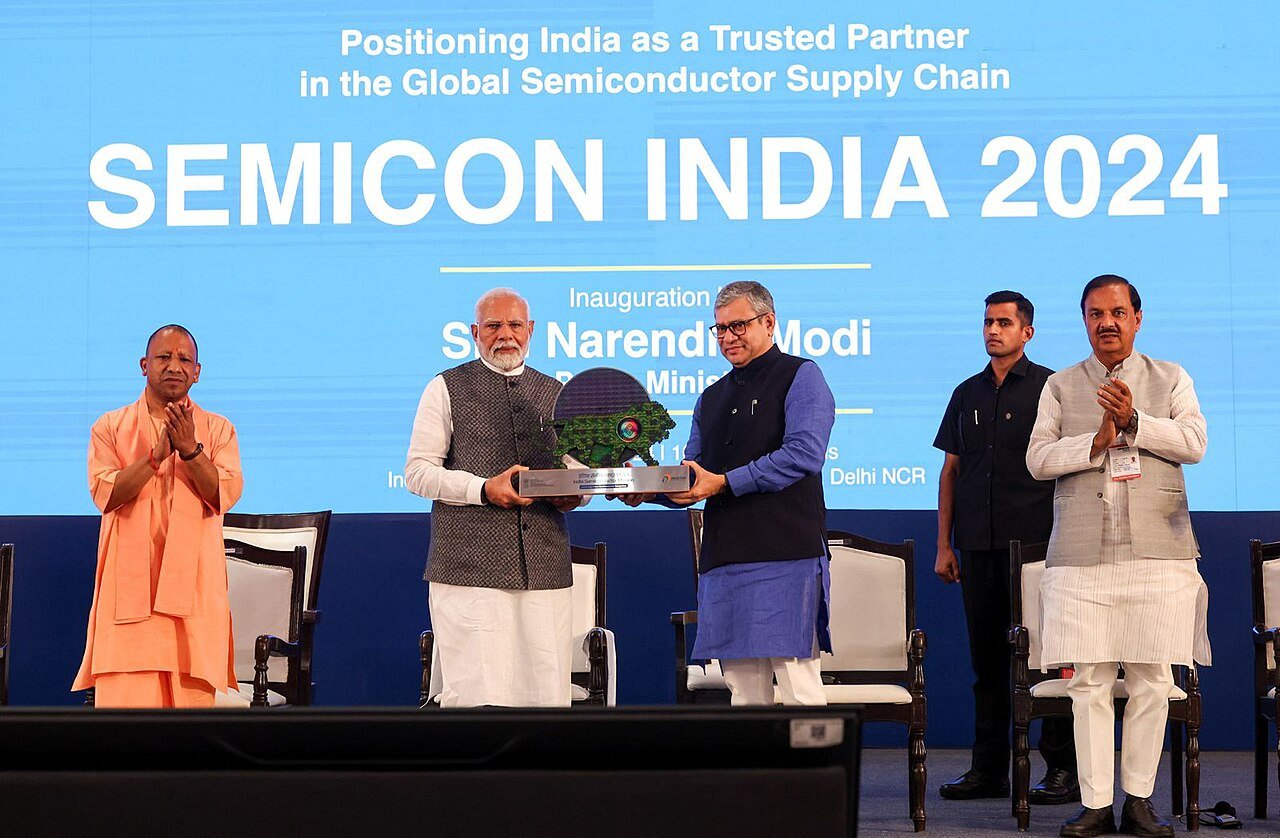
Three projects in one day. Tata Electronics and Taiwan’s PSMC get approval for India’s first commercial silicon fab at Dholera, about ₹91,000 crore, 50,000 wafer starts a month. Tata also gets a ₹27,000 crore packaging plant at Jagiroad, Assam, and CG Power with Japan’s Renesas and Thailand’s Stars Microelectronics a ₹7,600 crore unit at Sanand.
Foxconn walks out of Vedanta
Foxconn exits its chip joint venture with Vedanta. The pair had signed a ₹1.54 lakh crore MoU with Gujarat in September 2022, the largest announcement of the new push. It was never approved under ISM. Two other 2022 fab applications, from ISMC (with Tower) and IGSS, also stalled.
Micron: the first yes
The US memory maker commits to an assembly and test plant in Sanand, total outlay over ₹22,500 crore, with most of the cost shared by the Centre and Gujarat. Ground is broken in September 2023. It is the first project approved under the India Semiconductor Mission.
₹76,000 crore and a mission
After the global chip shortage, the Cabinet approves the ₹76,000 crore Semicon India Programme, offering up to 50 percent fiscal support for fabs, display fabs, compound semiconductors and packaging, plus a Design Linked Incentive scheme. The India Semiconductor Mission is created to run it.
The chip shortage
Pandemic lockdowns, a surge in electronics demand and concentrated supply produce a worldwide chip shortage. Car plants halt for want of cheap microcontrollers. For India, which imports almost all its chips, semiconductors become a question of economic security.
The 2014 fabs die quietly
The government cancels the Letter of Intent issued to the HSMC consortium, which had failed to submit required documents despite several extensions. The Jaiprakash consortium had already withdrawn. The cancellation becomes public only in January 2019.
Two fabs approved on paper
After an Empowered Committee set up in 2011 and in-principle approval on 12 September 2013, the Cabinet clears two fabs: Jaiprakash Associates with IBM and Tower (₹34,399 crore, Yamuna Expressway, UP) and HSMC with STMicroelectronics and Silterra (₹29,013 crore, Prantij, Gujarat). Each is to make 40,000 wafers a month at 90 nm down to 28 or 22 nm, with interest-free loans of about ₹5,124 crore each.
The first fab incentive scheme
India’s first semiconductor policy offers capital subsidies to attract fabs. No commercial fab is built under it.
SCL leaves industry for strategy
SCL is placed under the Department of Space in 2005 and renamed the Semi-Conductor Laboratory in 2006. From now on its job is strategic chips for ISRO and defence, not the mass market.
India becomes the design back office, then more
Intel, AMD, Qualcomm, Nvidia, NXP and others build large Indian design and verification teams. India becomes central to how the world’s chips are designed, even as almost none are made there.
SCL restarts
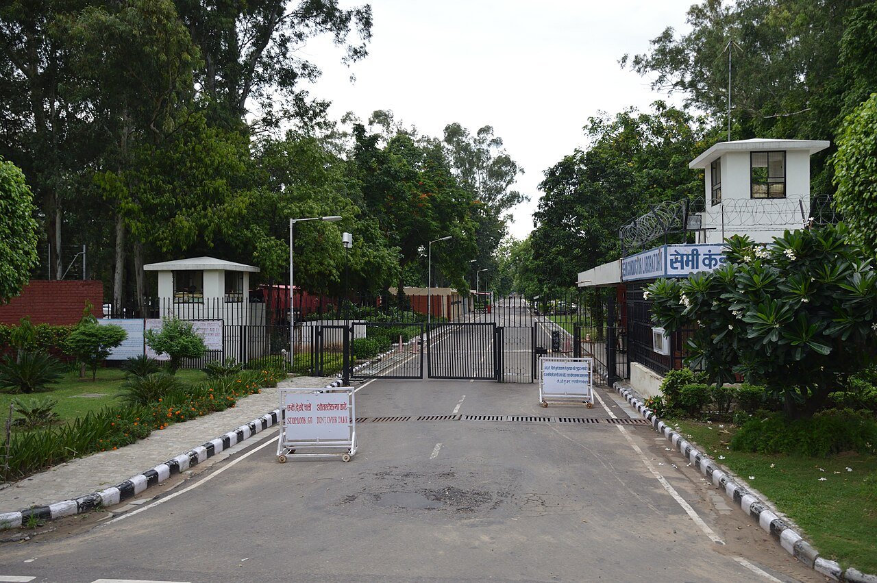
Eight years after the fire, SCL resumes production. By then the global frontier has moved from about 1 micron to around 0.25 micron, and Taiwan’s foundries are pulling away.
The Mohali fire
A fire destroys SCL’s main production line. As of 2022, published accounts still describe the cause as a mystery, including whether it was accidental. The real cost is time: India loses eight years of production in the decade the world industry scales up.
TSMC is founded
Morris Chang founds TSMC as a pure-play foundry that only manufactures chips designed by others. The model lets chip companies go fabless and concentrates manufacturing in Taiwan.
Texas Instruments comes to Bangalore
Texas Instruments opens a design centre in Bangalore, among the first multinational R&D centres in India. It is the start of the design strength that would define India’s semiconductor story for 35 years.
5-micron chips, made in India
With technology from American Microsystems Inc., SCL begins commercial production of 5-micron CMOS chips on 4-inch wafers for telecom, clocks, calculators and defence. According to a surviving SCL technical record, it later moves through 3, 2 and 1.2 micron toward 0.8 micron capability.
The Cabinet says yes to SCL
The Union Cabinet approves Semiconductor Complex Limited, to be built at Mohali, Punjab, as a vertically integrated chip maker for strategic and commercial electronics.
Strategic electronics first
Public-sector Bharat Electronics and government labs work with discrete semiconductor devices for defence and communications. They build capability, but not a commercial integrated-circuit industry.
India’s Semiconductor Race at a Glance
| Year | Milestone | What it meant |
|---|---|---|
| 1976 | SCL approved | India commits to its own fab |
| 1984 | 5-micron CMOS production | A few years behind the frontier |
| 1985 | Texas Instruments, Bangalore | Design era begins |
| 1987 | TSMC founded | Foundry model changes the industry |
| 1989 | SCL fire | Eight lost years |
| 1997 | SCL restarts | World has moved on |
| 2005-06 | SCL to Space Department | Strategic, not commercial |
| 2014 | Two fabs approved | Both dead by 2018 |
| 2021 | ₹76,000 crore mission | Ecosystem approach |
| 2022-23 | Vedanta-Foxconn collapses | Money alone is not enough |
| 2023 | Micron Sanand approved | First project under ISM |
| 2024 | Tata fab, Tata Assam, CG, Kaynes | Fab and packaging together |
| 2025 | HCL-Foxconn and four more | Spread to UP, Odisha, Punjab, AP |
| Feb 2026 | Micron ships | First made-in-India memory modules |
| Jul 2026 | Semicon 2.0 | ₹1,27,500 crore, six pillars |
| Sep 2026 | Five units producing | All packaging; fab due 2028 |
India’s 12 Approved Semiconductor Projects
Status as of 28 September 2026. Investment figures are approved amounts.
| Project | Location | Type | Approved | Status |
|---|---|---|---|---|
| Micron | Sanand, Gujarat | Memory ATMP | Jun 2023 | Producing (Feb 2026) |
| Tata Electronics + PSMC | Dholera, Gujarat | Silicon fab, 28-110 nm | Feb 2024 | Under construction; due 2028 |
| Tata Semiconductor Assembly and Test | Jagiroad, Assam | OSAT | Feb 2024 | Under construction |
| CG Semi (with Renesas, Stars) | Sanand, Gujarat | OSAT | Feb 2024 | Producing |
| Kaynes Semicon | Sanand, Gujarat | OSAT | Sep 2024 | Producing |
| HCL-Foxconn | Jewar, UP | Display driver chips | May 2025 | Under construction |
| SiCSem | Odisha | Silicon carbide fab | Aug 2025 | Under construction |
| 3D Glass Solutions | Odisha | Advanced packaging | Aug 2025 | Under construction |
| CDIL | Mohali, Punjab | Discrete devices ATMP | Aug 2025 | Producing (Sep 2026) |
| ASIP Technologies | Andhra Pradesh | OSAT | Aug 2025 | Under construction |
| Crystal Matrix | Dholera, Gujarat | GaN micro-LED display fab | May 2026 | Approved |
| Suchi Semicon | Surat, Gujarat | OSAT | May 2026 | Producing (Sep 2026) |
Seven stages, and where India’s projects sit
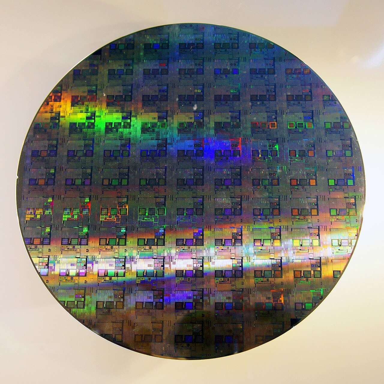
Micron’s Sanand plant and Tata’s Dholera fab are not rival versions of the same factory. Open each stage.
1. Design
2. Wafer fabrication (the fab)
3. Wafer test
4. Dicing
5. Assembly and packaging
6. Final test
7. Into products
Design (strong) → Fab (starting) → Package and test (producing) → Tools and materials (Semicon 2.0)
Semicon 2.0: The Six Pillars
₹1,27,500 crore, approved 15 July 2026.
Semicon 1.0 paid mostly for factories. The government’s own September 2026 backgrounder says Semicon 2.0 “adds machines and materials, design, research and talent to the mission”, so that the chain runs from raw materials to finished chips, “and not merely its closing stages”.
| Pillar | What it funds | Starting point |
|---|---|---|
| 1. Design | Indian chip IP, chip and system designs | 105 start-ups developing chips |
| 2. Machines and materials | Tool makers, chemicals, gases, materials | Almost no local base |
| 3. More fabs | Silicon, compound, discrete and display fabs | First fab due 2028 |
| 4. ATMP/OSAT | Advanced packaging technologies | Five units producing |
| 5. R&D | Nodes beyond 28 nm, with global labs | 28-110 nm today |
| 6. Talent | Chip design, cleanroom and fab-construction skills | ~68,000 students trained, 315 universities |
Does India Need the Smallest Chips?
The headline race is about 3 nm and 2 nm processors for phones and AI servers, and in 2026 Taiwan makes nearly all of them. India’s first fab starts at 28 nm to 110 nm. That sounds far behind, and in pure technology terms it is.
But most chips in the world are not leading-edge. Microcontrollers in cars, power-management chips, display drivers, sensors and telecom parts use mature nodes, and the 2020-21 shortage was mostly a shortage of exactly these cheap parts. Starting there gives a new fab real customers. Semicon 2.0’s R&D pillar then aims to push toward more advanced nodes with partners inside and outside India.
The Next Test
Approvals were the easy part.
Can Dholera start on time? The government’s date for the first fab is 2028. Fabs routinely slip; a new fab in a new country is harder still.
Can it reach good yields? A fab that produces too many defective chips loses money on every wafer. Yield is learned over years, which is why partners like PSMC matter.
Will suppliers come? A fab needs hundreds of local suppliers of gases, chemicals and spare parts. That is exactly what the machines-and-materials pillar is meant to attract.
Will Indian chip IP sell? The DLI start-ups have designs; the test is whether they win global customers.
Will policy last? Every earlier attempt faded. A fab takes years to pay back, so support has to outlast political and technology cycles.
🤔 Did You Know?
- SCL’s Mohali fab still makes strategic chips: government releases credit it with a camera chip on Chandrayaan-3‘s lander and radiation-hardened chips on Aditya-L1.
- India spent almost USD 150 billion on chip imports between FY17 and FY25, according to a September 2026 government backgrounder.
- The 2014 fab plans promised about 22,000 direct jobs. None materialised.
- CDIL’s new commercial line brought production back to Mohali, 42 years after SCL’s first chips there.
Quiz: Can You Beat India’s Semiconductor Timeline?
Tap a question to reveal the answer.
1. When did SCL begin commercial 5-micron CMOS production?
2. What happened at SCL on 7 February 1989?
3. Which strength did India build while fabs lagged?
4. When was the ₹76,000 crore Semicon India Programme approved?
5. Who is building India’s first commercial wafer fab?
6. What does ATMP stand for?
7. How big is Semicon 2.0?
Explore More Timelines
People Also Ask
Frequently Asked Questions
Related AiTimeline Stories
⚠️ Editorial Note
Checked against PIB releases of February 2014, February, July and September 2026, the India Semiconductor Mission, Wikipedia’s Semi-Conductor Laboratory entry, and news reports of the May 2026 approvals and the September 2026 production launches. Several points in circulating summaries were corrected or added: SCL was approved in 1976 and moved to the Department of Space in 2005 (renamed in 2006), and to MeitY in 2023; the Crystal Matrix and Suchi approvals of 5 May 2026 that took the total to 12; the failed Vedanta-Foxconn venture; and the government’s own 2028 date for the first fab. The cause of the 1989 fire has never been established and no cause is suggested here. Investment and capacity figures are approved or planned, not achieved; only the five units named were in commercial production at the time of writing. This is editorial, AI-assisted content.
Sources & further reading
Every dated entry above was checked against these references. Last reviewed 28 September 2026.
- PIB: India Building Semiconductor Future (17 September 2026)
- PIB: Cabinet approves Semicon 2.0 (15 July 2026)
- PIB: PM to inaugurate Micron ATMP facility in Sanand (27 February 2026)
- PIB: Approval to establish two semiconductor wafer fabs (14 February 2014)
- Business Standard/PTI: Govt cancels permit granted to HSMC Tech
- Upstox News: Cabinet nod for Crystal Matrix and Suchi Semicon (May 2026)
- Communications Today: Five semiconductor units operational (September 2026)
- Wikipedia: Semi-Conductor Laboratory
- India Semiconductor Mission