Applied Materials India: Accelerating Chip Ecosystem Growth
Applied Materials India from a 2002 Bengaluru start to 300-mm wafer validation and a USD 5bn Vision 2035 pledge: what it does and why it matters for chips.
Latest Story
India is building chip plants. But who builds the machines that make the chips? One of the biggest answers is Applied Materials, the Silicon Valley company whose tools deposit, etch and inspect the layers inside almost every modern chip. It came to Bengaluru in 2002 as an engineering centre. It then added university labs, a 300-mm wafer validation centre in 2024 and a 8.06 lakh sq ft campus in January 2026. On 17 September 2026 it pledged USD 5 billion over ten years under India Vision 2035. This is the full timeline of Applied Materials India, what the company actually does, and what its plans can and cannot do for India’s chip ecosystem.
💡 Short Answer
Applied Materials, the world’s second-largest chip-equipment maker, has operated in India since 2002. Its Bengaluru teams design, simulate and validate tools used in fabs worldwide. In 2023 it planned a USD 400 million collaborative engineering centre. In 2024 it opened the India Validation Center, which can process 300-mm wafers. On 17 September 2026 it pledged USD 5 billion over ten years (Vision 2035), including a proposed 140-acre research park and a tenfold increase in India-based supply-chain capacity.
Applied Materials in India: Key Questions
Applied Materials India in Ten Lines
- 1967: Applied Materials is founded in California to supply chip-making equipment and materials.
- 2002: Applied Materials India opens in Bengaluru as an engineering centre.
- 2005 onwards: IIT Bombay partnership builds India’s first university 200-mm fab facility.
- 2023: Coatings research with IIT Patna and IIT Ropar.
- June 2023: USD 400 million collaborative engineering centre announced; 40+ suppliers and institutes engaged by July.
- March 2024: India Validation Center opens and processes 300-mm wafers.
- September 2024: ASCENT research programme and a Tamil Nadu MoU for a Chennai AI centre.
- January 2026: 8.06 lakh sq ft ITPL workplace opens.
- 17 September 2026: USD 5 billion Vision 2035, a 140-acre research park, and a 10x supply-chain target.
- Still ahead: Indian suppliers qualified for global tools, and fabs at volume to use them.
What Does Applied Materials Actually Do?
The company behind the machines, not the chips.
A chip is built layer by layer. Films a few atoms thick are deposited, patterned, etched away, implanted, polished and measured, hundreds of times. Applied Materials makes the tools for most of those steps. It calls itself a materials-engineering company: its job is to control what is added to and taken off a wafer at atomic scale.
It does not make chips, and it does not make the lithography scanners that print the patterns, which are ASML’s field. That split matters for India. A fab such as Tata’s Dholera plant will buy tools from several makers. Applied’s opportunity is to be one of them, and to build more of the tools’ parts, software and engineering in India.
By revenue Applied is the world’s second-largest chip-equipment supplier, behind ASML. Its biggest product lines are deposition and etch, followed by inspection and metrology, ion implantation, planarisation and, increasingly, packaging tools for AI chips.
From sand to server: where does Applied fit?
Tap each stage. Applied’s name is not on your phone’s chip, but its machines touch many of these steps. Some steps belong to other companies, and that matters too.
Why India, and Why Now?
The first reason was people. In 2002 Bengaluru offered software, hardware and data engineers at scale. Applied’s Indian teams began with engineering support and grew into product design, simulation and testing. The company now says Indian engineers work on almost every new product it makes.
The second is customers. Until 2023 India had no chip plants to sell to. By September 2026 it had 12 approved units worth about ₹1.64 lakh crore, five of them producing, and a silicon fab due in 2028. Equipment makers follow fabs.
The third is geopolitics. Chip-tool makers are under pressure to spread their engineering and supply chains beyond a few countries. In February 2026 Applied agreed to pay a USD 252 million US penalty over past exports to China. India, with engineers, a government subsidy programme and good relations with Washington, fits the diversification story.
The fourth is policy. Semicon 2.0, approved in July 2026, explicitly funds machines and materials. Two months later Applied’s Vision 2035 put a number on its side of that equation.
From one centre to a ten-year programme
June 2023
- USD 400 million over four years
- One collaborative engineering centre, Bengaluru
- 500+ engineering jobs, 2,500 ecosystem jobs (projected)
- 40+ suppliers and institutes engaged
- Equipment subsystems and components
- No mission-backed chip plant producing yet
Sept 2026
- USD 5 billion over about ten years
- Proposed 140-acre research park with cleanrooms
- R&D headcount to more than double (reported)
- India supply-chain capacity to grow 10x by 2035
- R&D, ecosystem and talent pillars
- 5 mission-backed plants producing; a fab due 2028
Applied Materials India Timeline: 1967 to 2026
Newest first. Announcements, facilities and partnerships.
Vision 2035: USD 5 billion for India
On the day Prime Minister Narendra Modi opens SEMICON India 2026, Prabu Raja, president of Applied’s Semiconductor Products Group, announces Applied Materials India Vision 2035: a USD 5 billion investment over the next decade. It has three pillars: deepen R&D in India, accelerate the ecosystem, grow talent. The centrepiece is a proposed 140-acre advanced semiconductor research park with cleanrooms and collaborative R&D with customers and suppliers. Applied also aims to grow its India-based supply-chain capacity tenfold by 2035. Reports add that it plans to more than double its Indian R&D headcount and has proposed a customer-support centre in Gujarat.
Semicon 2.0 puts machines on the agenda
The Cabinet approves Semicon 2.0 with ₹1,27,500 crore. Semicon 1.0 mainly paid for factories. The new phase adds machines and materials, design, R&D and talent, which are the layers equipment makers work in. Under Semicon 1.0, 12 units worth about ₹1.64 lakh crore were approved. By 17 September 2026 five of them were in commercial production, all of them packaging plants.
An 8.06 lakh sq ft Bengaluru workplace
Applied Materials India opens a new 8.06 lakh square foot workplace at ITPL, Whitefield. The ribbon is cut by Prabu Raja, HR chief Joji Gill and Avi Avula, president of Applied Materials India, with Karnataka’s industries commissioner Gunjan Krishna. The company describes it alongside its other Indian facilities: the India Validation Center, a Class 1K cleanroom for inspection, prototyping and component qualification, and the Chennai AI centre.
A bet on advanced packaging
Applied buys 9% of BE Semiconductor Industries (Besi), the Dutch packaging-equipment maker, becoming its largest shareholder. The two had worked together since 2020 on die-to-wafer hybrid bonding, which joins chips copper to copper and is becoming important for AI processors and memory stacks.
ASCENT and the Chennai AI centre
Tamil Nadu and Applied Materials India sign an MoU in San Francisco, with Chief Minister M.K. Stalin and Prabu Raja present, for a Centre of Excellence in AI and Data Science in Chennai, aimed at semiconductor manufacturing and equipment. Applied says it will create more than 500 technical jobs in the state. On 10 September Applied India launches ASCENT, an annual research programme. Its first partners are IIT Kharagpur, IIT Hyderabad and IIT Gandhinagar, working on power, materials, chemical delivery, sensors, vacuum components, automation and sustainability.
India Validation Center opens
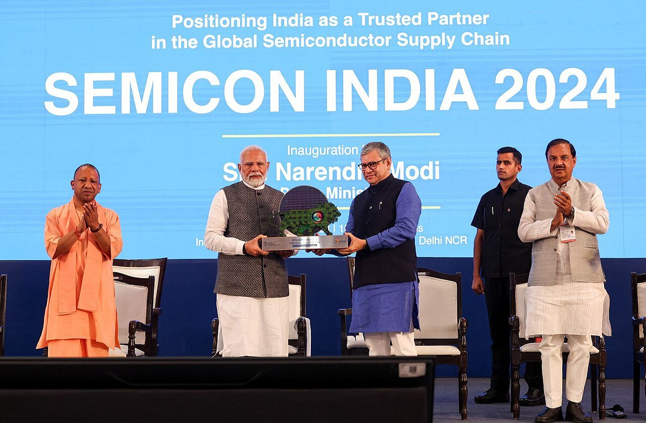
IT minister Ashwini Vaishnaw commissions the India Validation Center (IVC). It supports early pilots, process engineering, lab management and supplier and academic collaboration, and it can design, characterise and qualify semiconductor equipment from end to end. Applied says it demonstrated 300-mm wafer processing there, a first for private industry in India. It now calls the IVC India’s first and only 300-mm semiconductor R&D facility.
40+ suppliers and institutes sign up
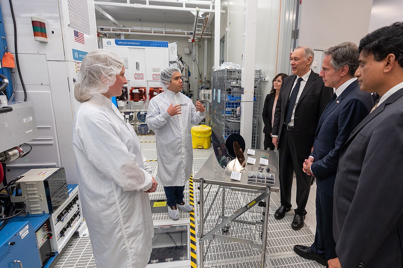
A month after the announcement, Applied says it has engaged more than 40 suppliers and academic institutions for the planned centre. Suppliers would use Applied’s equipment and processes to test and validate their own parts, so they can go from design to qualified supplier without building a fab of their own.
USD 400 million collaborative engineering centre
Applied says it will build a collaborative engineering centre in Bengaluru to develop and commercialise chip-equipment technology alongside global and Indian suppliers and research institutes. It plans a gross investment of USD 400 million over four years, and projects 500+ engineering jobs, potentially 2,500 more in the manufacturing ecosystem, and more than USD 2 billion of planned investment supported in the centre’s first five years. The same visit brings Micron’s Sanand plant, India’s first approved chip project.
Coatings research at IIT Patna and IIT Ropar
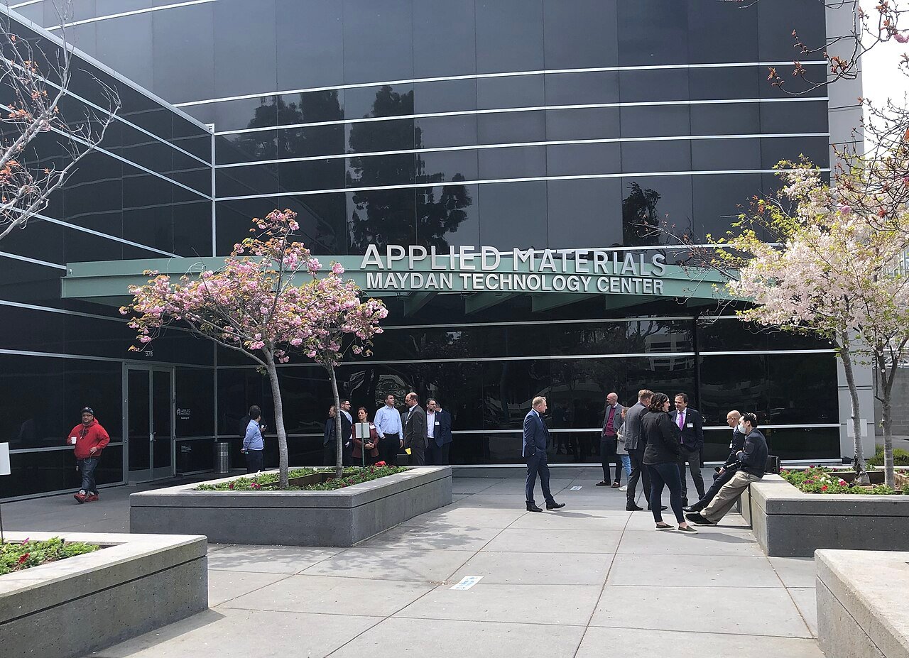
Applied India starts a three-year programme with IIT Patna on wear- and corrosion-resistant coatings. In June it announces a centre of excellence in thermal-spray coatings at IIT Ropar, co-funded with Metallizing Equipment Company. Both have support from the Department of Science and Technology’s Advanced Manufacturing Technologies programme.
IIT Bombay: a university fab
Applied’s partnership with IIT Bombay starts with a few sponsored projects in 2005. Over the next decade it grows into India’s first university-based facility with 200-mm fab tools, three labs for nanotechnology, chemistry and materials science, and a jointly offered semiconductor technology and manufacturing certification programme.
Applied Materials India is founded
Applied Materials sets up its Indian subsidiary, drawn by the software, hardware and engineering talent in Bengaluru. It starts as an engineering and IT centre. Over two decades it takes on product design, simulation, testing and validation, until Indian teams work on almost every new product the company makes.
A Silicon Valley start
Michael McNeilly and four partners found Applied Materials to supply chemical vapor deposition systems and specialty materials to early chipmakers. It lists on NASDAQ in 1972. After James Morgan becomes CEO in 1976, the company refocuses on chip equipment. By 2026 it is the world’s second-largest equipment supplier by revenue, behind ASML.
Applied Materials India at a Glance
| Date | Milestone | Why it matters |
|---|---|---|
| Nov 1967 | Applied Materials founded | Chip-equipment and materials business begins |
| 2002 | Applied Materials India set up | India joins the product-engineering network |
| 2005 | IIT Bombay partnership begins | Leads to a university 200-mm fab facility |
| Apr 2023 | IIT Patna coatings programme | Materials research for tool parts |
| Jun 2023 | USD 400m engineering centre; IIT Ropar CoE | Suppliers, academia and engineers in one place |
| Jul 2023 | 40+ suppliers and institutes engaged | Domestic supplier base starts forming |
| Mar 2024 | India Validation Center | 300-mm wafer processing in India’s private sector |
| Sep 2024 | ASCENT; Tamil Nadu AI CoE MoU | University research and AI for fabs |
| Apr 2025 | 9% Besi stake (global) | Hybrid bonding for advanced packaging |
| Jan 2026 | 8.06 lakh sq ft ITPL workplace | Room for a larger India workforce |
| Jul 2026 | Semicon 2.0 (government) | Machines and materials become policy |
| 17 Sep 2026 | Vision 2035: USD 5 billion | Research park, 10x supply chain, talent |
Applied’s Facilities in India
What exists, and what is only planned. Status as of 28 September 2026.
| Facility | Place | What it does | Status |
|---|---|---|---|
| ITPL workplace (8.06 lakh sq ft) | Whitefield, Bengaluru | Engineering and innovation teams | Open (Jan 2026) |
| India Validation Center | Bengaluru | Equipment design, characterisation, qualification; 300-mm wafers | Open (Mar 2024) |
| Class 1K cleanroom | Bengaluru | Inspection, prototyping, component qualification | Open |
| AI and Data Science CoE | Chennai | AI for high-volume manufacturing and equipment design | Operating (MoU Sep 2024) |
| Engineering offices | Mumbai, Pune | Engineering and support | Open |
| Collaborative engineering centre | Bengaluru | Co-development with suppliers and academia | Announced 2023; spending not disclosed |
| 140-acre research park | Bengaluru (reported) | Cleanrooms and R&D with customers and suppliers | Proposed (Sep 2026) |
| Customer-support centre | Gujarat | Support for fabs and packaging plants | Proposed (reported) |
Why 300-mm Matters, and What the IVC Is Not
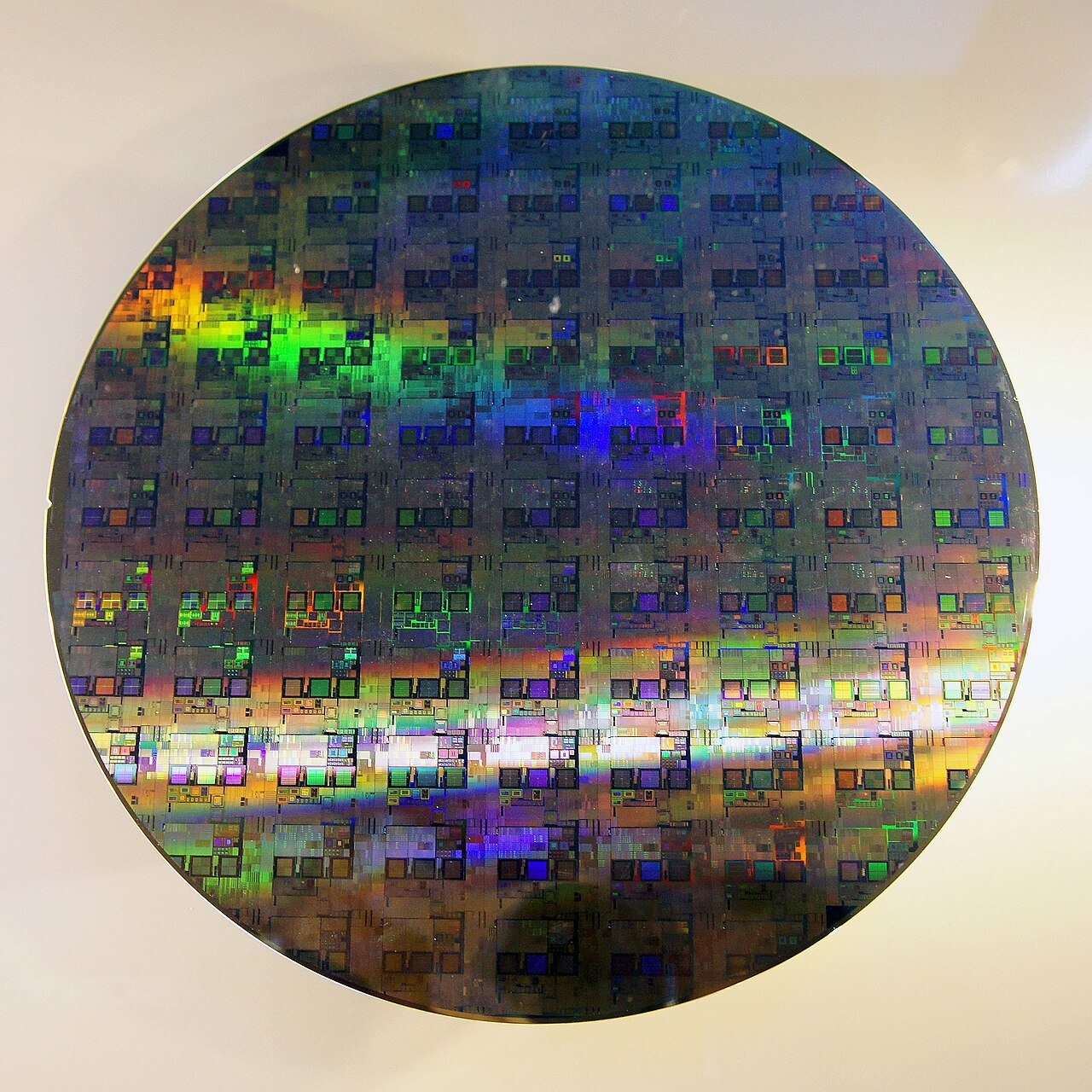
A 300-mm wafer is about 12 inches across and holds more than twice as many chips as a 200-mm wafer. Almost all leading-edge and most mature high-volume fabs run on 300 mm, including the Tata-PSMC fab being built at Dholera. An equipment lab that can run 300-mm wafers can test tools and parts under conditions close to a real fab.
That is what the India Validation Center does. It is not a chip factory. A commercial fab runs tens of thousands of wafers a month to sell chips. The IVC runs wafers to prove that a chamber, a part or a process works. Both are needed. Until 2024, the second kind of work on 300-mm wafers had to happen outside India’s private sector.
Six blocks. Which one can India build alone?
Tap a block to see where India stands, what Applied is doing there, and what is still missing.
Applied’s University Partners in India
Research programmes with published dates.
| Institution | Since | Focus |
|---|---|---|
| IIT Bombay | 2005 | 200-mm fab tools facility, materials labs, manufacturing certification |
| IIT Patna | Apr 2023 | Wear- and corrosion-resistant coatings (3-year programme) |
| IIT Ropar (with Metallizing Equipment Co.) | Jun 2023 | Thermal-spray coatings centre of excellence |
| IIT Kharagpur, IIT Hyderabad, IIT Gandhinagar | Sep 2024 | ASCENT: power, materials, chemical delivery, sensors, vacuum, automation, sustainability |
| Tamil Nadu institutions | Sep 2024 | AI, machine learning and data science for equipment |
Applied has also worked with IISc Bengaluru on advanced-materials applications. The pattern is the same in each case. A chip-design engineer can learn on a laptop. A process or equipment engineer needs cleanroom hours, real chambers and real failure modes, and these programmes give students some of that before they reach a fab.
The Missing Layer: Suppliers
An etch or deposition tool is made of thousands of parts: vacuum pumps, valves, gas-delivery panels, RF power supplies, ceramic and quartz chamber parts, sensors, robots and software. Today almost none of these are made in India for global chip tools.
Applied’s 2023 plan tried to change that by letting suppliers design, test, validate, modify and qualify their parts on Applied’s equipment in Bengaluru. Vision 2035 turns it into a target: ten times the India-based supply-chain capacity by 2035, from Indian suppliers and from global ones that move here.
If it works, the payoff goes beyond Applied. A qualified Indian supplier of chamber parts can sell to other tool makers and to the fabs themselves. That is how clusters in Taiwan, Korea and Singapore were built.
What Applied Can and Cannot Do for India
✅ Can
- Design and validate equipment in India
- Qualify Indian suppliers for global tools
- Train engineers on real 300-mm processes
- Fund university research on equipment problems
- Support Indian fabs and packaging plants as a supplier
❌ Cannot
- Build or run India’s fabs
- Guarantee that any Indian fab reaches good yield
- Replace lithography, wafers, gases or chemicals from other firms
- Create demand for chips made in India
- Turn a pledge into a supply chain without real orders
What Success Would Look Like by 2035
A built research park. The 140-acre site is a commitment in September 2026. The first test is land, construction and cleanrooms on a visible schedule.
Indian parts inside global tools. The 10x supply-chain target should show up as named Indian suppliers shipping qualified components.
Fabs at volume. Equipment ecosystems grow around running fabs. Dholera’s 2028 start and the ramp of India’s packaging plants matter as much as Applied’s own spending.
Engineers who move into fabs. ASCENT, IIT Bombay and the Chennai centre should produce process and equipment engineers, not only software and design talent.
R&D that starts here. The real shift would be new processes and tools invented in Bengaluru and shipped worldwide, which is what Raja meant by “inventions done here must scale globally”.
🤔 Did You Know?
- Applied’s first business in 1967 was chemical vapor deposition, and deposition is still one of its biggest product lines.
- IIT Bombay’s 200-mm facility, built with Applied, is described as India’s first university-based facility with 200-mm fab tools.
- Vision 2035’s USD 5 billion is 12.5 times the USD 400 million Applied pledged in 2023.
- The new ITPL workplace has an art installation on the ground floor that tells the company’s sand-to-silicon materials story.
Quiz: How Well Do You Know the Chip Machine Makers?
Tap a question to reveal the answer.
1. What does Applied Materials mainly sell?
2. When was Applied Materials India founded?
3. What is special about the India Validation Center?
4. How much did Applied pledge under Vision 2035?
5. Which IITs were in ASCENT’s first edition?
6. What does Semicon 2.0 add to India’s chip programme?
Explore More Timelines
People Also Ask
Frequently Asked Questions
Related AiTimeline Stories
⚠️ Editorial Note
Checked against Applied Materials’ India press releases, its PR Newswire release on ASCENT, Reuters and trade-press coverage of Vision 2035 (17-18 September 2026), trade-press reports of the ITPL opening (28 January 2026), PIB releases on Semicon 2.0, and Applied’s Wikipedia entry. Corrections to circulating summaries: the 2023 plan was USD 400 million, not ₹400 million; the Bengaluru campus is 8.06 lakh sq ft and opened in January 2026; the Tamil Nadu MoU was signed in September 2024; the IIT Bombay partnership dates from 2005; and the USD 5 billion Vision 2035 plan of September 2026 was added. Investment and job figures are company projections, not audited spending. AiTimeline has no commercial relationship with Applied Materials. This is not investment advice.
Sources & further reading
Every dated entry above was checked against these references. Last reviewed 28 September 2026.
- Reuters: Applied Materials to invest $5 billion in India (17 September 2026)
- Indian Startup News: Applied Materials India Vision 2035 (18 September 2026)
- Business Today: Applied Materials to invest $400 million over four years (June 2023)
- Applied Materials: India Validation Center commissioned (March 2024)
- PR Newswire: Applied Materials India launches ASCENT (10 September 2024)
- Indian Startup News: Applied Materials AI and Data Science CoE in Tamil Nadu (September 2024)
- BW Businessworld: Applied Materials CoE with IIT Ropar (June 2023)
- Dataquest: Applied Materials unveils 8.06 lakh sq ft Bengaluru workplace (January 2026)
- Evertiq: Applied Materials acquires 9% stake in Besi (April 2025)
- PIB: Cabinet approves Semicon 2.0 (15 July 2026)
- Wikipedia: Applied Materials