TSMC: How Taiwan Semiconductor Became a Global Chip Powerhouse
TSMC history from Morris Chang's 1987 pure-play foundry to 2nm chips, CoWoS for AI, a US$265B Arizona plan and fabs in Japan and Germany. Full timeline.
Latest Story
Some of the world’s most important chips are designed by companies that do not make them. The processor in an iPhone, the GPU in an AI server and many custom accelerators are drawn up in California and elsewhere, then manufactured in Taiwan by one company. This TSMC history traces how Morris Chang’s 1987 idea of a pure-play foundry grew into a chipmaker with 534 customers, a 2nm process in volume production and a US$265 billion plan in Arizona.
💡 Short Answer
TSMC became a global chip powerhouse by doing one thing: manufacturing chips for other companies and never competing with them. Founded by Morris Chang on 21 February 1987, it turned that trust into scale, took the process lead around the 7nm generation in 2018, and began 2nm volume production in late 2025. In 2025 it earned about US$122 billion from 534 customers.
TSMC History: Key Questions
TSMC in Nine Points
- The idea was the invention: in 1987 Morris Chang built a chip factory that would never sell its own chips.
- It began small and state-backed: a joint venture of Taiwan’s government, Philips and private investors, in a 6-inch fab leased from ITRI.
- It enabled the fabless industry: NVIDIA, Qualcomm, AMD after 2009 and Apple’s chip team all design without owning a leading-edge fab.
- Early firsts: 0.18-micron copper (December 1999) and the first full-scale 300mm fab at 0.13 micron (2001).
- The lead: TSMC moved ahead of Intel around 7nm in 2018 and has shipped each node since on a steady cadence to 2nm in 2025.
- Packaging became a weapon: CoWoS and InFO, once niche, are now as critical to AI chips as the transistors.
- Scale in 2025: 534 customers, 12,682 products, 305 technologies, about US$122 billion revenue.
- 2026 is a record year: Q2 revenue of US$40.2 billion, 66% from HPC, and growth guided above 40%.
- Going global: Arizona (US$265 billion plan), Kumamoto and Dresden, while Taiwan keeps the most advanced production.
The 1987 Idea: You Design It, We Build It
Why a factory that sells no chips changed the industry.
By the 1980s a chip company needed two very different skills: designing circuits and running a factory full of clean rooms, lithography tools and process engineers. Almost every chipmaker did both. A brilliant design team without a fab had to beg spare capacity from a rival, which could see its designs and might compete with it.
Morris Chang saw the gap. Born in 1931, he spent 25 years at Texas Instruments before Taiwan’s government invited him in 1985 to lead the Industrial Technology Research Institute (ITRI). Taiwan had a pilot chip line at ITRI but no company able to compete with the U.S. and Japanese giants on design. Chang’s answer was a company that would not design at all.
The pure-play foundry model: TSMC manufactures chips designed by its customers and does not design, manufacture or market semiconductor products under its own brand.
How TSMC describes its business model in its annual reports
The pitch was trust. A customer handing TSMC a new processor design knew the factory had no processor of its own to protect. That made TSMC the natural partner for the fabless companies that multiplied from the late 1980s, and later for giants that chose to stop running leading-edge fabs, such as AMD, which spun off its factories in 2009.
You have designed a billion-dollar chip. Which factory do you choose?
This is the question at the heart of TSMC’s 1987 idea.
Tap A, B or C.
Follow one AI accelerator from idea to data centre. Tap each stage.
This is a simplified path for a typical modern AI chip. The logo on the finished part belongs to the designer. The factory is someone else.
Question: NVIDIA designed the chip. Who manufactured the silicon?
Think about it, then tap Reveal.
The Node Race: 3 Microns to 2 Nanometres
Each dot is a generation TSMC brought to volume production.
The Full TSMC Timeline, 1987 to 2026
Newest first. Entries tagged 2026 cover this year’s developments.
2026
2nm target raised to 120,000 wafers a month2026
TSMC now plans about 120,000 2nm wafers a month by the end of 2026, up from an earlier estimate of 100,000, reports say, after Apple, NVIDIA, AMD, Qualcomm and MediaTek raised 2nm orders by 10 to 20 percent. Five fabs are ramping the node at once, two in Hsinchu and three in Kaohsiung. First-year 2nm output is described as 45% higher than 3nm’s first year in 2023.
Record months and US$29.4 billion more capex2026
The board approves about US$29.4 billion of capital spending for advanced technology, packaging and real-estate capacity. On 10 September TSMC reports August revenue of NT$514.81 billion, up 10.1% on July and 53.3% on August 2025. Industry trackers expect 3nm to overtake 5nm as TSMC’s biggest revenue node in the second half.
2026
Record quarter and another US$100 billion for Arizona2026
Second-quarter revenue reaches US$40.20 billion, up 33.7% year on year, with a 67.7% gross margin and net income up 77.4%. High-performance computing is 66% of revenue; 3nm is 30% of wafer revenue, 5nm 33% and 2nm 3%. C.C. Wei announces another US$100 billion for Arizona, taking the state total to US$265 billion for fabs at 2nm and below, packaging and R&D. The 2026 capex budget rises to US$60–64 billion and full-year growth guidance to slightly above 40%.
2026
2025 annual report: 534 customers, 12,682 products
TSMC’s 2025 figures: 12,682 products for 534 customers on 305 process technologies, capacity above 17 million 12-inch-equivalent wafers, and 74% of wafer revenue from 7nm and below. Revenue was NT$3,809.05 billion (about US$122.4 billion), up 31.6%, and net income NT$1,717.88 billion (about US$55.2 billion), with a 59.9% gross margin.
2025
2nm enters volume production
TSMC’s N2 process enters volume production on schedule, with “good yield” in C.C. Wei’s words. It is TSMC’s first nanosheet (gate-all-around) transistor, replacing the FinFET used since 16nm. The company discloses the milestone quietly on its website rather than with a launch event. N2P and A16, with backside power delivery, follow in 2026.
2025
US$100 billion more for Arizona, announced at the White House
Standing with President Trump, C.C. Wei announces at least US$100 billion more for three additional Arizona fabs, two advanced packaging plants and an R&D centre, lifting TSMC’s Arizona commitment to US$165 billion, then the largest single foreign direct investment in U.S. history.
2024
Arizona, Kumamoto and Dresden: the global network arrives
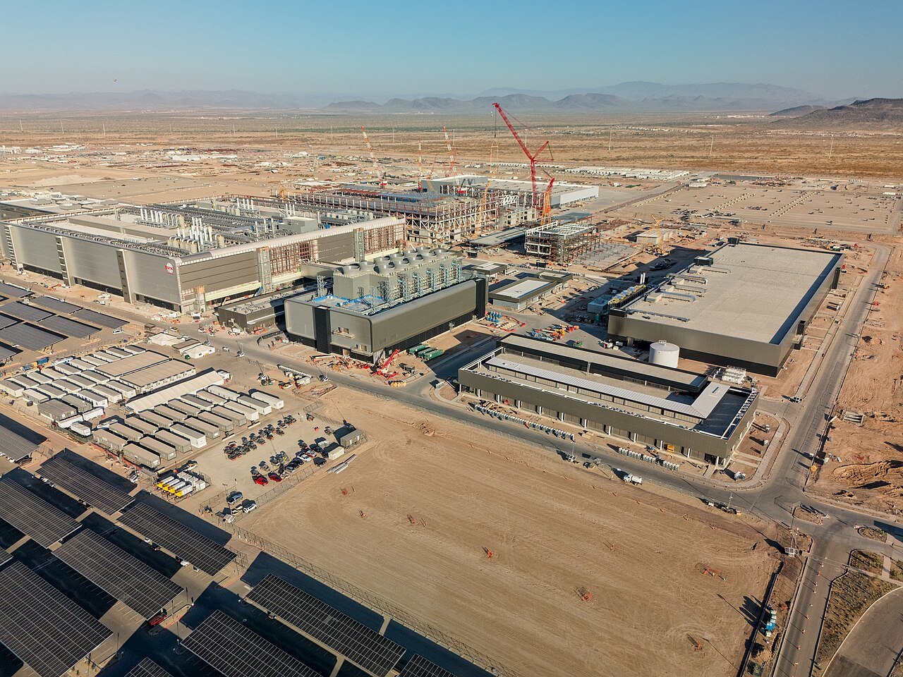
TSMC’s first Arizona fab enters high-volume 4nm production, and in November the U.S. finalizes up to US$6.6 billion in CHIPS Act grants. In Japan, the JASM fab in Kumamoto, built with Sony, Denso and Toyota, begins volume production at the end of the year. In Germany, ESMC, with Bosch, Infineon and NXP, broke ground in Dresden on 20 August.
C.C. Wei becomes chairman and CEO
After six years as CEO under chairman Mark Liu, C.C. Wei takes both top jobs as the AI boom turns TSMC into one of the world’s most valuable companies. Advanced packaging capacity, not transistors, becomes the tightest bottleneck, and TSMC races to multiply CoWoS output.
2022
3nm volume production
TSMC marks 3nm volume production with good yields at Fab 18 in Tainan. Three weeks earlier, on 6 December, President Biden visited the Arizona site as TSMC raised its U.S. plan to two fabs and about US$40 billion. 3nm grows into the workhorse for iPhone processors and, from 2025, AI accelerators.
5nm, Arizona, and the Huawei cut-off
N5 enters volume production in the second quarter. On 15 May TSMC announces its first Arizona fab, a US$12 billion plan. From 15 September, U.S. export rules bar it from supplying Huawei, then one of its largest customers. For the first time, geopolitics shapes TSMC’s customer list and its map.
7nm leadership, and Morris Chang retires
7nm enters volume production in the second quarter with more than 40 customer tape-outs by year-end, for phones, GPUs, CPUs, AI and game consoles. Around this generation TSMC moves ahead of Intel in process technology. On 5 June 2018, Morris Chang, 86, retires; Mark Liu becomes chairman and C.C. Wei CEO.
10nm, and InFO wins Apple outright
10nm enters volume production, and 16nm passes 20% of wafer revenue. TSMC’s InFO wafer-level packaging debuts in the Apple A10 in the iPhone 7, helping TSMC become Apple’s sole A-series supplier. Packaging becomes a competitive weapon, a decade before the AI rush makes it critical.
Apple’s A8 and a 54% market share
TSMC makes Apple’s A8 processor on 20nm, the start of a partnership that shapes the next decade. Its 16nm FinFET Plus passes full reliability qualification. That year it ships 8.26 million 12-inch-equivalent wafers, serves 453 customers with 8,876 products, and estimates its foundry share at 54%.
CoWoS and the 28nm platform
TSMC brings CoWoS (Chip-on-Wafer-on-Substrate) to production, first for Xilinx’s Virtex-7 FPGAs, which join several dies on a silicon interposer. At the same time, GIGAFAB Fab 15 ramps 28nm quickly and becomes a long-lived platform, while 16nm FinFET development begins. CoWoS looks niche for years; in the 2020s it becomes the heart of every big AI accelerator.
Morris Chang returns as CEO
Four years after handing the CEO job to Rick Tsai, Chang, 77, takes it back during the global financial crisis. He raises capital spending into the downturn instead of cutting it, a bet that pays off at 40nm and 28nm. TSMC also launches its Integrated Sign-Off Flow for 65/55nm and, later, 40nm and 28nm, easing customers’ path from design to working silicon.
The world’s first full-scale 300mm fab
TSMC announces that Fab 12 is the world’s first full-scale 12-inch (300mm) fab producing 0.13-micron chips with production-worthy yields. Construction had begun in 1999. A 300mm wafer has about 2.25 times the area of a 200mm one, and many process steps are done per wafer, so cost per chip falls.
0.18-micron, copper, and two acquisitions
TSMC offers a true 0.18-micron process from May 1999, and on 7 December 1999 becomes the first pure-play foundry to formally offer a commercial 0.18-micron copper process. Copper wiring conducts better than aluminium as interconnects shrink. In 2000 TSMC buys Worldwide Semiconductor (WSMC) and TSMC-Acer, widening its lead over rival UMC.
1997
First Taiwan company on the NYSE
TSMC’s American Depositary Shares begin trading on the New York Stock Exchange. U.S. investors can now fund the capital-hungry expansion, and the listing binds TSMC to U.S. disclosure rules, which is why so much of its history can be checked in SEC filings today.
WaferTech: TSMC’s first U.S. fab
In November 1995 TSMC and Altera announce a joint-venture fab in the U.S.; Analog Devices and Integrated Silicon Solution join in 1996, and the US$1.2 billion plant, WaferTech, is built in Camas, Washington. TSMC also opens its first 8-inch fab in Hsinchu in 1995. Arizona, a quarter-century later, is not TSMC’s first American factory.
Listed in Taipei
TSMC lists on the Taiwan Stock Exchange (stock code 2330). Semiconductor manufacturing never stops needing capital: each new process generation needs new tools, new fabs and new research. Public markets give TSMC a way to pay for the next one.
Close to the customers
A year after its founding, TSMC opens a North American subsidiary in Silicon Valley. Most of the chip designers it hoped to serve were in the U.S., and many of them, such as the young fabless firms of the late 1980s and early 1990s, could not afford a fab of their own.
1987
TSMC is founded
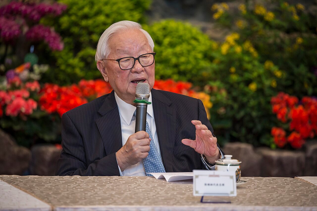
Morris Chang, a former Texas Instruments executive invited to run Taiwan’s ITRI in 1985, founds TSMC as a joint venture of the Taiwan government, Philips and private investors. Its first plant, Fab 1, is a 6-inch fab leased from ITRI. The idea: a pure-play foundry that makes chips for others and never competes with them. Many in the industry doubted anyone would outsource manufacturing.
TSMC by the Numbers
How the customer base and technology mix have grown.
| Measure | 2014 | 2019 | 2025 |
|---|---|---|---|
| Customers | 453 | 499 | 534 |
| Products | 8,876 | 10,761 | 12,682 |
| Advanced share of wafer revenue | 42% (28nm and below) | 50% (16nm and below) | 74% (7nm and below) |
| Foundry share (TSMC estimate / trackers) | 54% | about 50% | about two-thirds |
Two things stand out. First, TSMC is not only a 2nm company: it ran 305 distinct technologies in 2025, from specialty processes for car and sensor chips to the leading edge. Second, the money is concentrated at the top. In the second quarter of 2026, 77% of wafer revenue came from 7nm and more advanced nodes, and high-performance computing, mostly AI, provided 66% of all revenue. Smartphones were once TSMC’s biggest market; AI data centres now are.
From One Island to Three Continents
Where TSMC makes chips, as of September 2026.
| Site | Technology | Status (Sep 2026) |
|---|---|---|
| Taiwan (Hsinchu, Taichung, Tainan, Kaohsiung) | 2nm to mature; 4 GIGAFAB clusters | Core base; all leading-edge research and first ramps |
| Arizona, U.S. | 4nm now; 3nm, 2nm and A16 planned | Fab 1 in volume since Q4 2024; Fab 2 3nm due 2H 2027 |
| Kumamoto, Japan (JASM) | 12/16nm and 22/28nm; 3nm at Fab 2 | Fab 1 in volume since end 2024; Fab 2 due 2028 |
| Dresden, Germany (ESMC) | 28/22nm and 16/12nm | Under construction; production due 2H 2027 |
| Nanjing and Shanghai, China | 16nm/28nm and 8-inch mature nodes | Operating; limited by U.S. export controls |
| Camas, Washington, U.S. (WaferTech) | 8-inch mature nodes | Operating since the late 1990s |
Arizona is the headline. The first fab has made 4nm chips since late 2024, the second is due to start 3nm volume production in the second half of 2027, and the July 2026 expansion adds fabs for 2nm and below. Japan and Germany are different: they focus on mature and specialty nodes for cars and industry, where the most advanced process is not the most important one. A car can contain hundreds of chips, and few need 2nm.
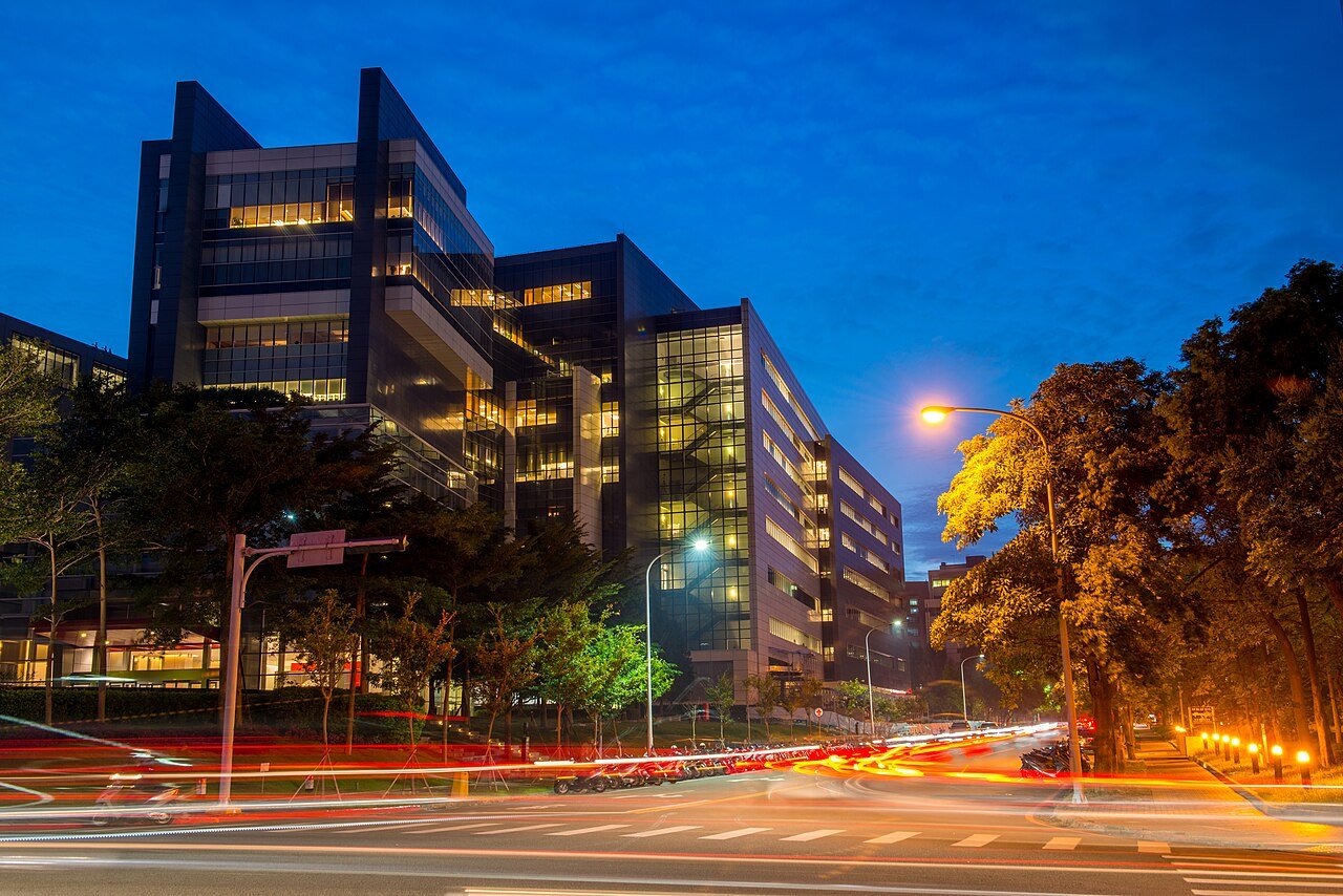
The research, the first ramp of every new node and most leading-edge output remain in Taiwan. Even with five fabs ramping 2nm in 2026, all five are in Hsinchu and Kaohsiung.
Why TSMC Matters to AI: Transistors Plus Packaging
A leading AI accelerator is not one chip. It is one or two very large logic dies, built on a process such as N4 or N3, placed next to stacks of high-bandwidth memory on a silicon interposer. TSMC’s CoWoS packaging does that joining. It first reached production around 2012 for Xilinx FPGAs and looked like a niche for years. From 2023, demand for AI chips made CoWoS capacity one of the tightest bottlenecks in the whole technology industry.
TSMC now groups its packaging under the name 3DFabric: CoWoS, InFO (first used in Apple’s A10 in 2016) and SoIC chip stacking. Its next logic steps target the same customers: A16 moves power wiring to the back of the wafer for data-centre chips, and A14 follows in 2028. The contest is no longer only about the smallest transistor, but about how much computing can be put into one package.
TSMC vs Samsung vs Intel: Different Models
Pure-Play vs Integrated
Who’s Who at TSMC
| Years | Leader | Role |
|---|---|---|
| 1987–2005 | Morris Chang | Founder, chairman and CEO |
| 2005–2009 | Rick Tsai | CEO; Chang stays chairman |
| 2009–2013 | Morris Chang | Returns as CEO in the financial crisis |
| 2013–2018 | Mark Liu and C.C. Wei | Co-CEOs; Chang chairman |
| 2018–2024 | Mark Liu (chair), C.C. Wei (CEO) | Chang retires 5 June 2018 |
| 2024– | C.C. Wei | Chairman and CEO |
Morris Chang
Ex-Texas Instruments, ITRI president from 1985, founded TSMC in 1987 and retired in 2018. Returned as CEO in 2009 to steer it through the financial crisis.
C.C. Wei
CEO since 2018 and chairman since June 2024. Led the AI-era expansion and the Arizona commitments of 2025 and 2026.
Mark Liu
Co-CEO from 2013 and chairman from 2018 to 2024, overseeing the 7nm, 5nm and 3nm generations.
Philips
The Dutch company held about 27.5% at the start and supplied process technology in TSMC’s first years.
ITRI
Taiwan’s Industrial Technology Research Institute, whose 6-inch pilot fab became TSMC’s Fab 1.
Apple and NVIDIA
Apple since the A8 in 2014; NVIDIA since the 1990s, now TSMC’s biggest AI customer.
The Risks
What TSMC itself lists, and what the market worries about.
- Geography. Most leading-edge output is in Taiwan, roughly 130 to 180 km across the Strait from mainland China. Any disruption there would hit phones, cars and AI data centres worldwide.
- Export controls. U.S. rules cut off Huawei in 2020 and limit what TSMC’s China fabs can do; rules can change again.
- Cost. Each node costs more to develop and build, and overseas fabs cost more to run than those in Taiwan.
- Power, water and earthquakes. Fabs use vast amounts of both, and Taiwan is seismically active.
- Concentration of demand. With 66% of revenue from HPC in Q2 2026, an AI spending slowdown would be felt quickly.
Did You Know?
- Arizona is TSMC’s second U.S. fab: WaferTech in Camas, Washington, opened in the late 1990s.
- Copper date: TSMC’s first commercial copper process was offered in December 1999, not 1998 as often repeated.
- The first 300mm fab: ground was broken in 1999, but full-scale production was announced in October 2001.
- Quiet milestone: 2nm volume production was announced on TSMC’s website, with no launch event.
- Chinese name: 台積電 (Tai Ji Dian), short for Taiwan Integrated Circuit Manufacturing.
Test Yourself: TSMC Quiz
1. When was TSMC founded?
2. Which European company was a founding partner?
3. What is a pure-play foundry?
4. When did TSMC first offer a commercial 0.18-micron copper process?
5. Where was TSMC’s first U.S. fab?
6. When did 2nm enter volume production?
7. What is TSMC’s total announced Arizona investment as of September 2026?
8. What is CoWoS?
Explore More Timelines
People Also Ask
Frequently Asked Questions
Related AiTimeline Stories
⚠️ Editorial Note
Company figures come from TSMC’s annual reports, Form 20-F filings and quarterly results, including the 2025 annual report (filed 16 April 2026) and Q2 2026 results (16 July 2026). U.S. dollar conversions of 2025 NT dollar figures are approximate. The 120,000-wafer 2nm target is as reported on 28 September 2026. Corrections to circulating summaries: TSMC’s first commercial 0.18-micron copper process was offered in December 1999, not 1998; its first full-scale 12-inch fab reached production in 2001, after ground was broken in 1999; WaferTech was set up in 1995–96 with Altera, ADI and ISSI; and the Arizona commitment is US$265 billion since July 2026, not US$165 billion. This article is not investment advice.
Sources & further reading
Every dated entry above was checked against these references. Last reviewed 29 September 2026.
- TSMC 2025 Annual Report
- TSMC: Second Quarter 2026 results (16 Jul 2026)
- CNBC: TSMC to invest additional $100 billion in Arizona (16 Jul 2026)
- TSMC: First commercially available 0.18-micron copper process (Dec 1999)
- TSMC: Fab12 world record for 0.13-micron on 300mm wafers (Oct 2001)
- TSMC: First Taiwan company to list on NYSE (1997)
- Focus Taiwan: TSMC officially begins 2nm volume production in Q4 2025
- TSMC: Up to US$6.6 billion CHIPS Act funding for TSMC Arizona
- TechPowerUp: TSMC to scale 2nm to 120,000 wafers per month by end of 2026
- TrendForce: Arizona 2nd fab 3nm in 2H27, Kumamoto in 2028 (Apr 2026)