Tata Dholera Fab: Every Stage of India’s First Commercial Chip Plant
Tata's Dholera fab, India's first commercial chip plant: ₹91,526 crore, PSMC and ASML, 50,000 wafers a month, and commercial output now due mid-2028.
Latest Story
The Tata Dholera fab in Gujarat is the plant meant to give India what it has tried and failed to build since 2011: a commercial factory that makes chips on silicon wafers, not just one that packages them. It is a ₹91,526 crore, 300 mm fab built with Taiwan’s PSMC, designed for 50,000 wafers a month on 28 to 110 nm processes. This page follows it from the empty Bhal plain to SEMICON India 2026, including the parts the launch headlines left out: the start date has moved from December 2026 to mid-2028, and production will begin at 55 and 90 nm, with 28 nm later.
💡 Short Answer
Tata Electronics is building India’s first commercial semiconductor fab at Dholera, Gujarat: a ₹91,526 crore, 300 mm plant with technology from Taiwan’s PSMC and lithography support from ASML, designed for 50,000 wafer starts a month on 28–110 nm processes. The Cabinet approved it on 29 February 2024 with 50% central support. Production will start at 55 and 90 nm, and the government now expects commercial operations in mid-2028, not December 2026 as first promised.
Tata Dholera Fab: Key Questions
The Dholera Fab in Ten Points
- A fab, not a packaging plant: Dholera makes the circuits on the wafer; India’s other new chip plants package and test.
- Approved 29 February 2024: ₹91,000 crore, 50,000 wafers a month, 28–110 nm.
- Fiscal Support Agreement, 5 March 2025: ₹91,526 crore project, 50% central support.
- Partners: PSMC licenses the processes (September 2024); ASML backs lithography (May 2026).
- The date moved: first chip promised for December 2026; commercial operations now mid-2028.
- The node moved: production starts at 55 and 90 nm, with 28 nm later.
- Soft ground: foundations were redesigned in 2025 for Dholera’s saline, silty soil.
- Third attempt: fabs backed in 2013–14 and the Vedanta–Foxconn plan of 2022 all fell through.
- The ecosystem is the second project: Merck, Sumitomo, Kelington, Sojitz, a 363-acre vendor park, ISM 2.0.
- The real test is yield and customers, not the building. No volume customer has been announced yet.
What a Fab Is, and Why India Did Not Have One
The difference between making chips and packaging them.
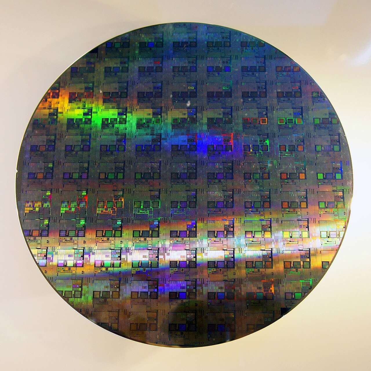
A chip starts as a polished disc of pure silicon. In a fab, that wafer goes through hundreds of steps over two to three months: thin films are deposited, patterns are printed by lithography, material is etched away, ions are implanted, metal wiring is laid down layer by layer. At the end, one 300 mm wafer carries hundreds or thousands of identical dies. All of it happens in a cleanroom far cleaner than an operating theatre, fed by ultra-pure water, specialty gases and stable power.
Those wafers then go to an OSAT (outsourced semiconductor assembly and test) or ATMP plant, which cuts them into dies, packages each one and tests it. That is the stage India has added fastest since 2023: Micron at Sanand, Kaynes and CG Semi in Gujarat, Tata at Jagiroad in Assam. Assembly plants matter, but they need wafers from somewhere else. A fab is what lets a country make the chip itself, and it costs roughly ten times as much.
India’s chip story before 2024 was largely design: tens of thousands of engineers at global chip companies in Bengaluru, Hyderabad and Noida designing chips that were fabricated in Taiwan, Korea or the United States. Dholera is the attempt to add the missing industrial layer.
🏭 Fab (front end): Dholera
- Deposition, lithography, etching
- Ion implantation, metallisation
- Hundreds of steps per wafer
- Output: finished wafers
- Cost: ~₹91,500 crore
🧩 OSAT/ATMP (back end): Sanand, Jagiroad
- Wafer dicing
- Die attach and wire bonding
- Packaging
- Final test
- Cost: a few thousand to ~₹27,000 crore
A fab is built in stages. Pick one to see where Dholera stands, what the last public evidence was, and what to check next.
Status as of 5 October 2026, from government and company statements and named reports.
Choose a stage above
The Date That Moved: December 2026 to Mid-2028
Every public target for Dholera’s first output, in the order it was stated.
When the foundation stone was laid in March 2024, Ashwini Vaishnaw said the first chip from Dholera would come out in December 2026, which would have been about 33 months from groundbreaking to silicon. That is fast even for experienced fab builders in Taiwan, and Dholera was a greenfield site on soft ground.
The date held in public until 2025. A Mint report in September 2025 said Tata expected its cleanroom to be ready only by early 2027, putting a first chip around mid-2027 and warning of rare-earth shortages. In March 2026 Vaishnaw said the first fab would be ready in 2028, and in July 2026 he told Reuters that commercial operations were expected in mid-2028.
Two things are worth separating. A first wafer through the line is a technical milestone; commercial production means yields and customer qualification good enough to sell. Many timelines blur the two. Even on the new date, Dholera would go from Cabinet approval to commercial output in a little over four years, close to what new fabs take elsewhere.
Tata Dholera Fab: The Full Timeline, 2009–2026
Newest first. Tags mark milestones reached, work in progress, dates that moved, and plans that did not happen.
2026
A 363-acre vendor park for 450 suppliers In progress
Tata Electronics is reported to be building a 363-acre plug-and-play supplier park beside the fab with Singapore’s Ascendas Firstspace, for about 450 domestic and international suppliers. The aim is to keep chemicals, gases, spare parts and maintenance crews minutes from the cleanroom, because a fab that waits days for a part loses wafers.
2026
SEMICON India: ‘aligned with government schedules’ In progress
At SEMICON India in New Delhi, Tata Electronics said construction at Dholera and its assembly plant at Jagiroad, Assam remained aligned with government schedules, with more than 450 ecosystem partners working on construction, chemicals, equipment and materials. CEO Randhir Thakur said the company planned 16 agreements at the show; those announced included Sumitomo Chemical (photoresists and high-purity chemicals such as hydrogen peroxide, IPA, ammonia water and sulphuric acid), Kelington of Malaysia (critical infrastructure and operational readiness), Enomoto, Sojitz with NRS (a chemical logistics network, signed 18 September) and L&T Semiconductor.
About 300 recent Indian graduates were training at PSMC’s fabs in Taiwan.
Start at 90 nm, commercial output mid-2028 Date moved
Bloomberg reported that Dholera would begin production mainly on the 90 nm process rather than 28 nm, the node the Tata Sons annual report for 2024–25 had highlighted. A Tata Electronics spokesperson said the plan had always been to start with 55 nm and 90 nm and then add 28 nm, which would remain a key part of its offering; PSMC said gradual introduction starting with mature nodes was normal.
IT minister Ashwini Vaishnaw told Reuters the fab was now expected to start commercial operations in mid-2028. In March 2024 he had said the first chip would come out in December 2026.
ISM 2.0: ₹1.27 lakh crore for the next phase Milestone
The Union Cabinet approves the second phase of the India Semiconductor Mission with an outlay of about ₹1.27 lakh crore over six years. Where the 2021 programme paid mainly for fabs and assembly plants, ISM 2.0 also covers semiconductor equipment, chemicals, gases, materials, chip design, R&D and talent: the supply chain Dholera needs around it.
2026
ASML signs on Milestone
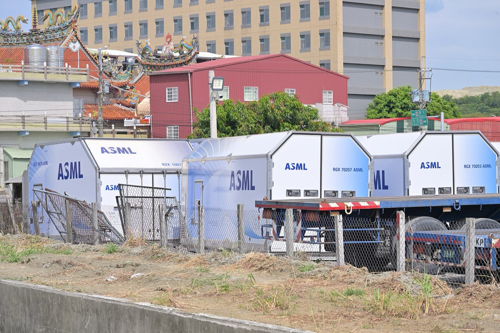
Tata Electronics and ASML, the Dutch company that makes the lithography machines every modern fab depends on, sign a memorandum of understanding during Prime Minister Modi’s visit to the Netherlands. ASML will support the establishment and ramp-up of Dholera with its ‘holistic suite’ of lithography tools and solutions, and the two will work on lithography training, R&D infrastructure and supply-chain resilience.
Why it matters: access to lithography tools and service is a gate no fab can bypass. Dholera’s mature nodes use deep-ultraviolet (DUV) tools, not the extreme-ultraviolet (EUV) machines used for leading-edge chips.
2026
Dholera fab SEZ notified Done
The Commerce Ministry notifies a special economic zone for Tata Semiconductor Manufacturing at Dholera, announced on 16 April as ‘India’s first chip fabrication plant’. It covers 66.166 hectares, with proposed investment of ₹91,000 crore and employment of 21,000. The zone was possible because SEZ rules were changed on 3 June 2025 to cut the minimum area for semiconductor SEZs from 50 to 10 hectares and allow sales into the domestic market on payment of duty.
2026
‘First fab by 2028’ Date moved
Opening Kaynes Semicon’s assembly plant at Sanand, Vaishnaw says four semiconductor plants will be ready in 2026, two more in 2027, and India’s first fab, at Dholera, in 2028. It is the first official sign that the December 2026 date has gone.
$735 million of bank loans Done
Tata Semiconductor Manufacturing signs about $735 million (around ₹6,835 crore) of loans from five foreign banks through their GIFT City branches, according to filings reported in March 2026. The lenders require Tata to keep majority ownership and the Tata brand. It is a small slice of a ₹91,526 crore project, but the first large external debt for it.
2025
Intel MoU: possible products for Dholera
Tata Electronics and Intel sign an MoU to explore manufacturing and packaging Intel products for Indian markets at the Dholera fab and the Assam assembly plant, and to work together on advanced packaging and AI PCs. It is an agreement to explore, not a wafer order, but it is the most prominent potential customer named so far.
Foundations redesigned for soft soil In progress
Reports say Tata has redesigned the fab’s foundations after studies found Dholera’s reclaimed land was clay-heavy, saline and silty, with low load-bearing capacity. Lithography and metrology tools need floors that barely move. Tata said it had engaged ‘world class experts’, including geotechnical firms Fugro and Cengers, and that the project remained on schedule.

Merck pact, and a rare-earth warning
At SEMICON India 2025 (2–4 September), Tata Electronics signs an MoU with Merck for high-purity materials, gas and chemical delivery systems and fab infrastructure services for Dholera. Days later Mint, citing unnamed executives, reports that Tata expects its cleanroom to be ready by early 2027, with tools and trial production to follow, and that shortages of rare earths and critical elements could delay a first chip targeted for mid-2027.
2025
Fiscal Support Agreement: ₹91,526 crore Milestone
The India Semiconductor Mission, Tata Electronics and Tata Semiconductor Manufacturing sign the Fiscal Support Agreement in the presence of Gujarat Chief Minister Bhupendra Patel. The project is valued at ₹91,526 crore; the Centre commits 50 percent of eligible project costs, released in step with Tata’s own spending. Thakur says construction is being undertaken ‘with a great sense of urgency’.
2024
PSMC definitive agreement Milestone
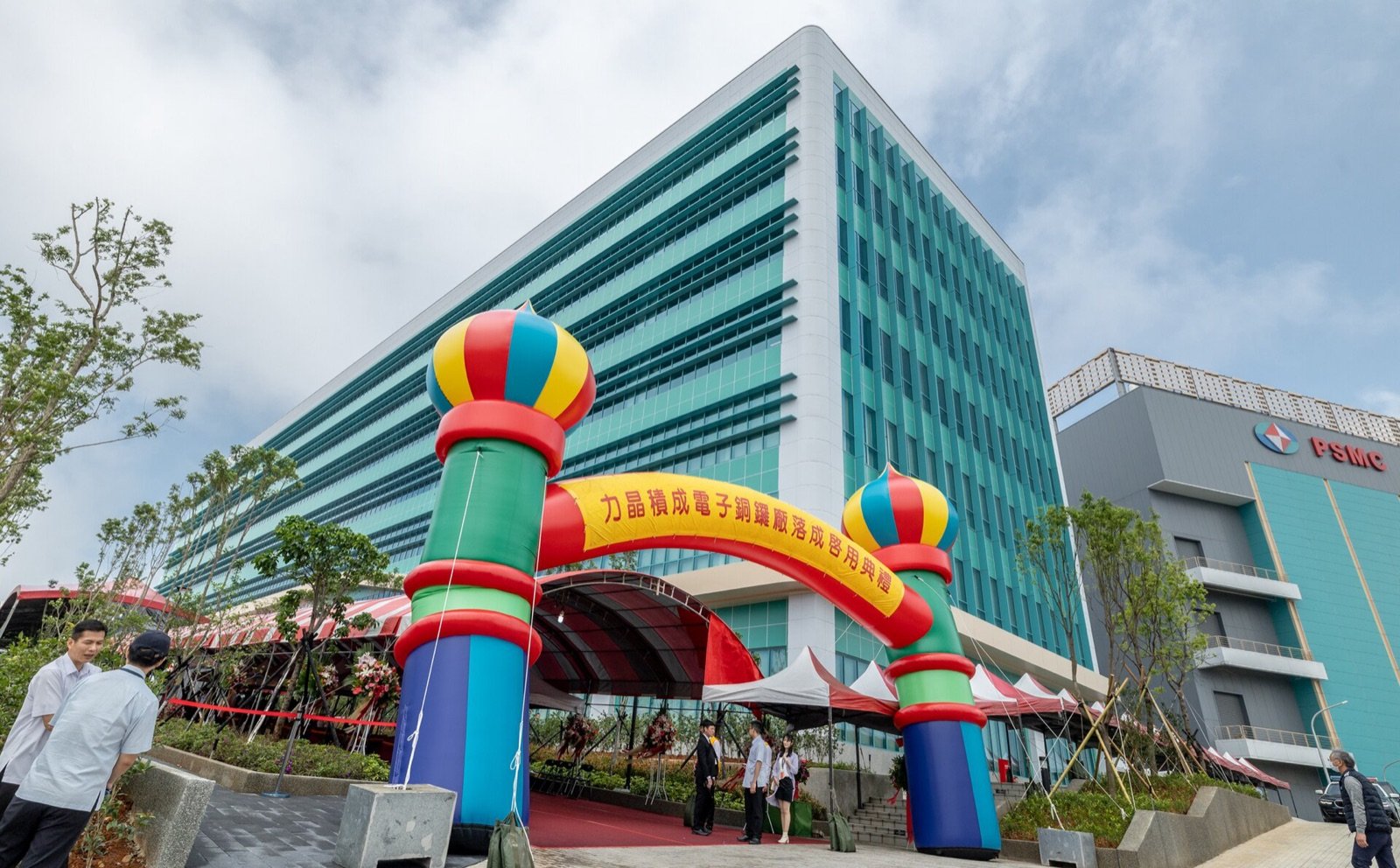
Tata Electronics completes its definitive agreement with Powerchip Semiconductor Manufacturing Corporation. PSMC will license a portfolio of process technologies from 28 nm to 110 nm, provide design and construction support for the greenfield fab, and give engineering support. Tata says its multi-fab vision for Dholera could eventually create more than 1,00,000 skilled jobs.
2024
Foundation stone; ‘first chip in December 2026’ Date moved
Prime Minister Modi lays the foundation stones of three semiconductor projects by video link from New Delhi at the ‘India’s Techade: Chips for Viksit Bharat’ event: Tata’s Dholera fab, Tata’s assembly and test plant at Morigaon, Assam, and CG Power’s assembly plant at Sanand, together worth about ₹1.25 lakh crore. Tata calls Dholera an AI-enabled fab. Vaishnaw says the first chip will come out in December 2026, a date that has since moved to 2028.
2024
Cabinet approves India’s first commercial fab Milestone
The Union Cabinet approves Tata Electronics’ proposal, with PSMC as technology partner, for a fab at Dholera with an investment of about ₹91,000 crore and capacity of 50,000 wafer starts a month. The planned nodes are 28 nm for high-performance computing, 40 to 110 nm for power-management chips, display drivers and microcontrollers. It is approved alongside two assembly plants.
2023
Foxconn quits Vedanta’s chip venture Did not happen
Foxconn says it is withdrawing from its semiconductor joint venture with Vedanta. The venture had signed an MoU with Gujarat on 13 September 2022 for a ₹1.54 lakh crore chip and display complex and chosen Dholera as its site, but had not secured a technology partner able to satisfy the government. Its exit leaves Dholera without a fab project until Tata.
2021
₹76,000 crore semiconductor programme Milestone
After the 2021 chip shortage idles car plants worldwide, the Cabinet approves a ₹76,000 crore programme for semiconductors and displays, offering fiscal support of up to 50 percent of project cost for fabs. The India Semiconductor Mission is set up to run it. This is the scheme that funds Dholera.
SPECS and PLI for electronics
The Scheme for Promotion of Manufacturing of Electronic Components and Semiconductors (SPECS) offers 25 percent capital support for electronic components, semiconductor and display fabrication, and assembly and test, alongside a production-linked incentive for phones. It builds India’s electronics assembly base but attracts no fab.
Two fabs approved, none built Did not happen
The government gives in-principle approval in September 2013, with letters of intent in 2014, to two consortia, each planning about 40,000 wafer starts a month, with nodes going down to 28 nm. One is led by Jaiprakash Associates with IBM and Tower Semiconductor; the other by HSMC Technologies with STMicroelectronics and Silterra, at Prantij in Gujarat. Jaiprakash pulls out, and HSMC’s letter of intent is cancelled in April 2018. Neither raised the money or locked in customers.
The ambition is written down
The government sets up an empowered committee in 2011 to find technology partners and investors for wafer fabs. The National Policy on Electronics, 2012 names fabs as a strategic goal. The words are in place twelve years before a fab is approved.
Dholera Special Investment Region
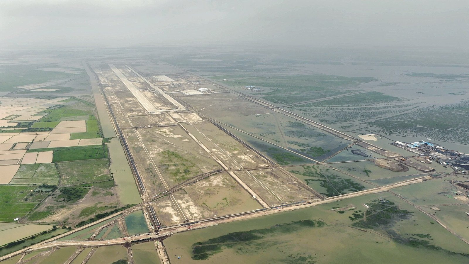
Gujarat designates Dholera, a flat, sparsely populated stretch of the Bhal region near the Gulf of Khambhat, as a Special Investment Region under its new SIR Act, and later as a node of the Delhi–Mumbai Industrial Corridor. For years it is mainly roads and plots. The fab makes it the centre of India’s chip plan.
90 nm Before 28 nm: What the Node Change Means
Not cutting-edge, and not meant to be.
In July 2026 Bloomberg reported that Dholera would start mainly at 90 nm, a process first used for high-volume chips about two decades ago, rather than the 28 nm highlighted in Tata Sons’ 2024–25 annual report. Tata said this was always the plan: start with 55 and 90 nm, then add 28 nm. PSMC said bringing up mature nodes first was normal.
Both things can be true. Starting with simpler processes lets a new team learn to run the fab, tune yields and qualify customers before attempting the harder node. And mature-node chips are not niche: power-management ICs, microcontrollers and display drivers ship in enormous volumes, and they are what ran short in 2021, idling car plants around the world. What 90 nm is not is a route into AI accelerators or smartphone processors, which need 5 nm or less and are made by TSMC, Samsung and Intel.
| Node | Typical chips | Where they go | When at Dholera |
|---|---|---|---|
| 90 nm | Power management, analog, microcontrollers | Cars, industrial gear, chargers | First, from 2027–28 |
| 55 nm | Microcontrollers, display drivers, mixed-signal | Phones, TVs, appliances, cars | First, from 2027–28 |
| 110 nm | Power and analog chips | Power supplies, motors, EVs | In licence; timing not stated |
| 40 nm | Logic, embedded memory | Connectivity, IoT, displays | In licence; timing not stated |
| 28 nm | Higher-performance logic | Computing, communications, cars | Later; ‘key part’ of plan |
The Dholera Fab by the Numbers
| Item | Dholera fab | Source |
|---|---|---|
| Owner | Tata Semiconductor Manufacturing (Tata Electronics) | PIB, Mar 2025 |
| Technology partner | PSMC, Taiwan | Tata, Sep 2024 |
| Lithography partner | ASML (MoU) | ASML, May 2026 |
| Project cost | ₹91,526 crore (~$11 billion) | PIB, Mar 2025 |
| Central support | 50% of eligible cost, pari-passu | PIB, Mar 2025 |
| Wafer size | 300 mm (12-inch) | Tata |
| Capacity | 50,000 wafer starts/month | PIB, Feb 2024 |
| Licensed nodes | 28, 40, 55, 90, 110 nm | PIB, Feb 2024 |
| Starting nodes | 55 and 90 nm | Tata, Jul 2026 |
| SEZ | 66.166 ha, notified 9 Apr 2026 | PIB, Apr 2026 |
| Jobs | 20,000+ direct and indirect | PIB, Mar 2025 |
| Commercial operations | Mid-2028 (target) | Vaishnaw, Jul 2026 |
Third Time: India’s Earlier Fab Attempts
Why 2013 and 2022 failed, and what is different now.
India’s first serious push came in 2013–14, when the government backed two consortia: Jaiprakash Associates with IBM and Tower Semiconductor near Greater Noida, and HSMC with STMicroelectronics and Silterra in Gujarat, each planning about 40,000 wafers a month. The technology partners were licensors, not investors, and neither group could raise the capital or line up customers. Jaiprakash pulled out and HSMC’s letter of intent was cancelled in 2018.
The second attempt was Vedanta–Foxconn, which signed a ₹1.54 lakh crore MoU with Gujarat in September 2022 and chose Dholera. It never found a technology partner the government would accept, and Foxconn left in July 2023.
Three things differ for Tata. The subsidy is larger and contractual: 50% of eligible cost from the Centre under a signed agreement, plus state support. The technology partner, PSMC, is a working foundry that is helping design and build the fab and train its staff, not just licensing a process. And the sponsor is a group with the balance sheet to carry a long build and a captive electronics business that can use the output. None of that guarantees yields or customers, which are what sank most new fabs elsewhere.
Why Dholera, and What the Site Costs
Dholera was chosen for land, not location. The Special Investment Region, designated in 2009, offered large contiguous plots, a state government willing to build roads, water and power to order, an airport under construction and space for suppliers. A fab also needs huge volumes of ultra-pure water and grid power that does not flicker: a split-second outage can scrap every wafer in process.
The cost of the site turned out to be underground. The Bhal region is flat, low-lying, saline land near the Gulf of Khambhat, and reports in November 2025 said Tata had redesigned the foundations after finding clay-heavy, silty soil with low load-bearing capacity. Lithography tools that print features a few hundred atoms wide cannot sit on a floor that settles. Tata said the redesign kept the project on schedule.
The Second Project: Building the Supply Chain
A fab consumes photoresists, high-purity acids and solvents, specialty gases, spare parts and service engineers every hour. Most of that supply chain sits in Japan, Taiwan, Korea, Europe and the US. Tata’s 2025–26 agreements are an attempt to bring parts of it to Gujarat: Merck for materials and gas and chemical delivery systems, Sumitomo Chemical for photoresists and high-purity chemicals, Kelington for critical infrastructure, Sojitz and NRS for chemical logistics, and a 363-acre vendor park for about 450 suppliers. The government’s ISM 2.0, approved in July 2026, adds incentives for equipment, materials and gases. Whether those suppliers actually set up plants near Dholera, rather than shipping from abroad, is one of the clearest measures of whether the fab becomes an industry.
Corrections to Claims Circulating Online
From the summary material this page was built from, and common in coverage.
“Production begins in 2027”
The government now says commercial operations in mid-2028 (Vaishnaw, July 2026). 2027 is when the cleanroom, tools and trial runs are expected.
“Chips from 110 nm to 28 nm”
That is the licensed range. Output starts at 55 and 90 nm; 28 nm comes later.
“Micron Sanand produces DRAM and NAND”
Sanand assembles, tests and packages memory chips. The memory wafers are made in Micron fabs abroad.
“Modi at the Dholera ceremony”
The March 2024 foundation stones were laid by video link from New Delhi, for three projects at once.
“Two fabs approved in 2014”
Approval in principle came in September 2013, letters of intent in 2014; neither fab was built.
2025–2026 setbacks and financing
Summaries skip the soil redesign, the rare-earth warning, the $735 million loans, the Intel MoU, ISM 2.0 and the 2028 date.
What Would Count as Success
Cleanroom and tools
Cleanroom qualified; ASML and other tools installed; first test wafers through the line.
Yield
Defect rates low enough on 90 and 55 nm to sell wafers at a profit after subsidy.
Commercial output
The government’s current target. Watch for named customers and volumes.
28 nm and full capacity
A 28 nm process in production and a ramp toward 50,000 wafers a month.
Local suppliers
Chemical, gas and parts makers producing near Dholera, not just warehousing imports.
Engineers who stay
Process and equipment engineers trained at PSMC running the line, and later starting the next fab.
Did You Know?
- Two months per wafer: a chip wafer can take 8 to 12 weeks to pass through all of a fab’s steps.
- Not India’s first fab: the government’s Semiconductor Laboratory at Mohali has made chips since the 1980s, on old, small-scale processes.
- Dholera’s first chip plan was Vedanta’s, not Tata’s, in 2022.
- 300 graduates were training in PSMC’s Taiwan fabs by September 2026.
- Lithography tools travel by air in many crates and take months to reassemble and qualify.
- ‘AI-enabled’: Tata says Dholera will use machine learning and data analytics for factory automation and yield.
Quick Quiz
1. What node will Dholera start production on?
2. When are commercial operations now expected?
3. Who licenses the process technology?
4. What is Micron’s Sanand plant?
5. Which company first picked Dholera for a chip plant?
Explore More Timelines
People Also Ask
Frequently Asked Questions
Where Dholera Stands
Two and a half years after approval, Dholera has its money, its technology licence, its lithography partner, its SEZ and a growing list of suppliers. What it does not yet have is a working cleanroom, installed tools, a single wafer or a named volume customer. The schedule has slipped about eighteen months from the first promise, and the first products will use the most mature processes in its licence.
That is not unusual for a first fab, and it is further than India has ever got. The milestones to watch are concrete: the first tool move-in, first wafers in 2027, a named customer, and commercial output by mid-2028. If those land, the larger prize is the people and suppliers the fab trains, which is what would make the next Indian fab cheaper and faster.
Related AiTimeline Stories
⚠️ Editorial Note
Last updated 5 October 2026. Approval, cost, capacity, node and SEZ figures come from Press Information Bureau releases; partnership details from Tata Electronics, ASML and PSMC statements; schedule changes from named reports (Bloomberg, Reuters, Mint) and ministerial remarks as reported. Targets are as stated and may change again. Nothing here is investment advice.
Sources & further reading
Every dated entry above was checked against these references. Last reviewed 5 October 2026.
- PIB: ISM, Tata Electronics and Tata Semiconductor Manufacturing sign Fiscal Support Agreement for Rs 91,526 crore Dholera fab (5 Mar 2025)
- PIB: Government notifies India's first chip fabrication plant at SEZ Dholera (16 Apr 2026)
- Tata Electronics: PSMC definitive agreement for technology transfer to build India's first fab (Sep 2024)
- Tata Group newsroom: Tata Electronics and ASML announce strategic partnership (16 May 2026)
- TrendForce: Tata's India fab to launch at 90nm; commercial production mid-2028 (20 Jul 2026)
- Business Standard: Not cutting-edge, but can Tata's chip fab reduce India's import bill? (23 Jul 2026)
- The Tribune (ANI): Tata Electronics set to sign 16 MoUs at SEMICON India 2026, CEO Randhir Thakur (Sep 2026)
- Electronics For You: Tata Electronics revises fab design for Dholera soil (28 Nov 2025)
- DigiTimes: Tata Semiconductor secures US$735 million for Dholera fab (24 Mar 2026)